Quantcast
Channel: op amp – Gas station without pumps
Viewing all 68 articles
Browse latest View live

Logarithmic amplifier

$
0
0

My son wanted to design a circuit to convert microphone inputs to loudness measurements usable by an Arduino (or other ATMega processor).  We discussed the idea together, coming up with a few different ideas.

The simplest approach would be to amplify the microphone then do everything digitally on the Arduino. There are several features of this approach:

  • The analog circuit is about as simple as we can get: a DC-blocking capacitor and an amplifier.  This would only need one op amp, one capacitor, and 2 resistors (plus something to generate a bias voltage—perhaps another op amp, perhaps a low-drop-out regulator).
  • Using digital processing, he can do true RMS voltage computation, and whatever low-pass filtering to smooth the result that he wants.
  • He can’t sample very fast on the ATMega processor, so high frequencies would not be handled properly.  He might be able to sample at 9kHz (about as fast as the ADC operates), but that limits him to 4.5kHz. For his application, that might be good enough, so this doesn’t kill the idea.
  • He’d like to have a 60dB dynamic range (say from 50dB to 110dB) or more, but the ADC in the ATMega is only a 10-bit converter, so a 60dB range would require the smallest signal to be ±½LSB, which is at the level of the quantization noise.  With careful setting of the gain for the microphone preamp, one might be able to get 55dB dynamic range, but that is pushing it a bit.  The resolution would be very good at maximum amplitude, but very poor for quiet inputs.

Although the mostly digital solution has not been completely ruled out, he wanted to know what was possible with analog circuits.  We looked at two main choices:

  • True-RMS converter chips (intended for multimeters).  These do all the analog magic to convert an AC signal to a DC signal with the same RMS voltage.  Unfortunately, they are expensive (over $5 in 100s) and need at least a 5v power supply (he is planning to use all 3.3v devices in his design).  Also true RMS is a bit of overkill for his design, as log(amplitude) would be good enough.
  • Using op amps and discrete components to make an amplifier whose output is the logarithm of the amplitude of the input.  Together we came up with the following block diagram:
Block diagram of the loudness circuit.

Block diagram of the loudness circuit. (drawn with SchemeIt).

We then spent some time reading on the web how to make good rectifier circuits and logarithmic amplifiers. I’ll do a post later about the rectifier circuits, since there are many variants, but I was most interested in the logarithmic amplifier circuits, which rely on the exponential relationship between current and voltage on a pn junction—often the emitter-base junction of a bipolar transistor.

My son wanted to know what the output range of the log amplifier would be and whether he would need another stage of amplification after the log amplifier. Unfortunately, the theory of the log amplifier uses the Shockley ideal diode equation, which needs the saturation current of the pn junction—not something that is reported for transistors.  There is also a “non-ideality” parameter, that can only be set empirically.  So we couldn’t compute what the output range would be for a log amplifier.

Today I decided to build a log amplifier and see if I could measure the output.  I also wanted to figure out what sort of dynamic range he could get from a log amp. Here is the circuit I ended up with, after some tweaking of parameters:
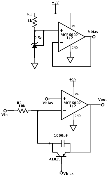
The top circuit is just a bias voltage generator to create a reference voltage from a single supply. I'm working off of 5v USB power, so I set the reference to 2.5v. He might want to use a 1.65v reference, if he is using 3.3v power. The bottom circuit is the log amplifier itself.

The top circuit is just a bias voltage generator to create a reference voltage from a single supply. I’m working off of 5v USB power, so I set the reference to 2.5v. He might want to use a 1.65v reference, if he is using 3.3v power.
The bottom circuit is the log amplifier itself.

I chose a PNP transistor so that Vout would be more positive as the input current got further from Vbias.  I have 6 different PNP transistors from the Iteadstudio assortment of 11 different transistors, and I chose the A1015 rather arbitrarily, because it had the lowest current gain. I should probably try each of the other PNP transistors in this circuit, to see how sensitive the circuit is to the transistor characteristics.  I suspect it is very sensitive to them.

The circuit only works if the collector-base junction is reverse-biased (the usual case for bipolar transistors), so that the collector current is determined by the base current. The emitter-base junction may be either forward or reverse biased.  Note that if Vin is larger than Vbias, the collector-base junction becomes forward-biased, the negative input of the op amp is slightly above Vbias, and the op amp output hits the bottom rail.

As long as Vin stays below Vbias, the current through R2 should be \frac{V_{bias} - V_{in}}{R_{2}}, and the output voltage should be V_{out}-V_{bias} = A \ln \frac{B(V_{bias} - V_{in})}{R_{2}} for some constants A and B that depend on the transistor. Note that changing R2 just changes the offset of the output, not the scaling, so the range of the output is not adjustable without a subsequent amplifier.

The 1000pF capacitor across the transistor was not part of the designs I saw on the web, but I needed to add it to suppress high-frequency (around 3MHz) oscillations that occurred. The oscillations were strongest when the current through R2 was large, and the log output high.  I first tried adding a base-emitter capacitor, which eliminated the oscillations, but I still has some lower-frequency oscillations when the transistor was shutting off (very low currents).  Moving the capacitor to be across the whole transistor as shown in the schematic cleaned up both problems.

I put ramp and sine wave inputs into the log amplifier.  The waveforms were generated with the Bitscope function generator, which does not allow setting the offset very precisely—there is only an 8-bit DAC generating the waveform.  Here is a sample waveform:
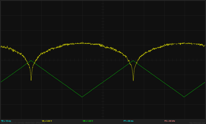
The green trace is the input, the yellow trace is the output.  The horizontal axis in the middle is at 2.5V for the input (so the input is always below 2.5V) and at 3V for the output.  THe scale is 1V/division for the input and 50mV/division for the output.

Click picture for larger image. The green trace is the input, the yellow trace is the output. The horizontal axis in the middle is at 2.5V for the input (so the input is always below 2.5V) and at 3V for the output. The scale is 1V/division for the input and 50mV/division for the output.  [And all those values should be visible in the saved snapshot, but they aren't.]

The ripple on the output is mainly artifacts of the low-resolution of the BitScope A-to-D converter—smoothing of multiple reads is done, but there is a lot of quantization noise. According to my analog scope there are still some 24MHz noise around, but it seems to be from the Vbias source—adding a 4.7µF capacitor between Vbias and +5V (adjacent pins on the op amp) cleaned things up a lot on the analog scope, without affecting the BitScope traces.

Using the cursors on the BitScope, I was able to measure the output voltages for input voltages of Vbias-0.5V, Vbias-1V, and Vbias-2.5V.  From these, I concluded that the scaling factor for the output was about 3.1–3.2 mv/dB.  The output was 3±0.07V, so the dynamic range is 140mV/(3.2 mv/dB), or about 44dB.  We can see the logarithmic response in an X-Y plot of the output vs the input:
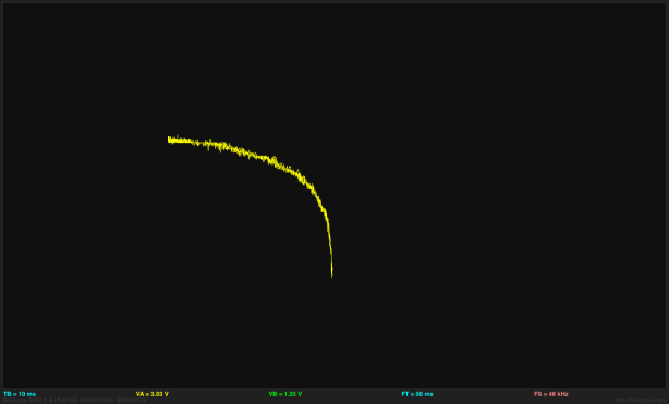
Output vs. input of the log amplifier.  Note that the output is the log of Vbias-Vin, so the log curve looks backwards here.

(Click for larger image) Output vs. input of the log amplifier. Note that the output is the log of Vbias-Vin, so the log curve looks backwards here.  It’s a shame that BitScope throws away the grid on XY plots, as the axes are still meaningful.

I also tried using an external oscillator, so that I could get better control of the offset voltage, and thus (perhaps) a better view of the dynamic range. I could fairly reliably get an output range of about 200mV, without the hysteresis that occurs when the collector-base junction gets forward biased. That would be over 60dB of dynamic range, which should be fine.

I should be able to adjust the voltage offset of the amplifier by changing R2. Increasing R2 reduces the current, which should lower the voltage. I tried several different values for R2 and measured the maximum output voltage, using the same input throughout:

1kΩ 3.106v
10kΩ 3.056v
100kΩ 2.992v
1MΩ 2.936v

The 60dB difference in current produces a 170mV difference in output, for 2.83 mV/dB.

Oops, those weren’t quite all the same, as the load from the resistor changes the input. Adding a unity-gain buffer driving the inputs and adjusting the input so that the output of the unity gain buffer has a slight flat spot at 0V gives me a new table:

1kΩ 3.12v
10kΩ 3.06v
100kΩ 3.00v
1MΩ 2.94v
5.6MΩ 2.90v

which is consistent with 3mV/dB. I was not able to extend this to lower resistances, as I started seeing limitations on the output current of the op amp. But it is clear that the amplifier can handle a 75dB range of current, with pretty good log response.

An Arduino input is about 5mV/count, so the resolution feeding the output of the log amplifier directly into the Arduino would be about 1.7dB/count. We could use a gain of 4 without saturating an op amp (assuming that we use 2.5V as the center voltage still), for about a 0.4 dB resolution. More reasonably, we could use a gain of 3 to get a resolution of about 0.54dB/count.

I tried that, getting the following table:

1kΩ 4.46v
10kΩ 4.28v
100kΩ 4.10v
1MΩ 3.91v
5.6MΩ 3.78v

This table is consistent with 9.1 mv/dB, for a resolution of about 0.54 dB/step on the Arduino.

I tried using the Arduino to collect the same data and fit with gnuplot:

The gnuplot fit agrees with the measurements made with the BitScope for 5 resistor values.  The resolution of the Arduino DAC limits the ability to measure the dynamic range.

(click plot to see larger version) The gnuplot fit agrees fairly well with the measurements made with the BitScope for 5 resistor values. The resolution of the Arduino DAC limits the ability to measure the dynamic range, and the cloud of points is broad enough to be consistent with slightly different parameter values.

The next thing for me to do on the log amp is probably to try different PNP transistors, to see how that changes the characteristics. My son will probably want to use a surface-mount transistor, so we’ll have to find one that is also available as a through-hole part, so that we can check the log amplifier calibration.


Filed under: Data acquisition Tagged: Arduino, BitScope, log amplifier, loudness, op amp

Logarithmic amplifier again

$
0
0

Yesterday, in Logarithmic amplifier, I ended with the following plot:

The gnuplot fit agrees with the measurements made with the BitScope for 5 resistor values.  The resolution of the Arduino DAC limits the ability to measure the dynamic range.

(click plot to see larger version) The cloud of points is broad enough to be consistent with slightly different parameter values.

I was bothered by the broad cloud of points, and wanted to come up with a better test circuit—one that would give me more confidence in the parameters.  It was also quite difficult to get close to Vbias—the closest this could measure was one least-significant-bit of the DAC away (about 5mV).  A factor of 512 from the largest to the smallest signal is 54dB, but only about the upper 40dB of that was good enough data for fitting (and very little time was spent at near the Vbias value).

I think that part of the problem with the cloud was that the input signal was changing fairly quickly, and the Arduino serializes its ADC, so that the input and output are measured about 120µsec apart.  I decided to use a very simple slow-changing signal: a capacitor charging toward Vbias through a large resistor.  My first attempt used a 1MΩ resistor and a 10µF capacitor, for a 10-second time constant:

Output voltage from log amplifier (with 3x gain in second stage) as capacitor charges. One fit uses the Arduino-measured Vin and Vbias voltages, the other attempts to model the RC charging as well. What are the weird glitches?

Output voltage from log amplifier (with 3x gain in second stage) as capacitor charges. (click picture for larger version) One fit uses the Arduino-measured Vin and Vbias voltages, the other attempts to model the RC charging as well. What are the weird glitches?

The capacitor charging should be a smooth curve exponential decay to Vbias, so the log amplifier output should be a straight line with time. There were two obvious problems with this first data—the output was not a straight line and there were weird glitches about every 15–20 seconds.

The non-straight curve comes from the capacitor not charging to Vbias. Even when the capacitor was given lots of time to charge, it remained stubbornly below the desired voltage. In think that the problem is leakage current: resistance in parallel with the capacitor. The voltage was about 1% lower than expected, which would be equivalent to having a 100MΩ resistor in parallel with the capacitor.  I can well believe that I have sneak paths with that sort of resistance on the breadboard as well as in the capacitor.

According to Cornell Dublier, a capacitor manufacturer, a typical parallel resistance for a 10µF aluminum electrolytic capacitor would be about 10MΩ [http://www.cde.com/catalogs/AEappGUIDE.pdf‎]:

Typical values are on the order of 100/C MΩ with C in μF, e.g. a 100 μF capacitor would have an Rp of about 1 MΩ.

So I may be lucky that I got as close to Vbias as I did.

The glitches had a different explanation: they were not glitches in the log amplifier circuit, but in the 5V power supply being used as a reference for the ADC on the Arduino board—I had forgotten how bad the USB power is coming out of my laptop, though I had certainly observed the 5V supply dropping for a second about every 20 seconds on previous projects.  The drop in the reference for the ADC results in a bogus increase in the measured voltages.  That problem was easy to fix: I plugged in the power supply for the Arduino rather than running off the USB power, so I had a very steady voltage source using the Arduino’s on-board regulator.

    With a proper power supply, I get a clean charge and the output is initially a straight line, but I'm still not getting close to Vbias.  Again the blue fit uses the measured Vin and Vbias voltages, while the green curve tries to fit an RC decay model. Note the digitization noise on the measured inputs towards the end of the charging time.

(click picture for larger version) With a proper power supply, I get a clean charge and the output is initially a straight line, but I’m still not getting close to Vbias. Again the blue fit uses the measured Vin and Vbias voltages, while the green curve tries to fit an RC decay model. Note the digitization noise on the measured inputs towards the end of the charging time.

To solve the problem of the leakage currents, I tried going to a larger capacitor and smaller resistor to get a similar RC time constant. At that point I had not found and read the Cornell Dublier application note, though I suspected that the parallel resistance might scale inversely with the capacitor size, in which case I would be facing the same problem no matter how I chose the R-vs-C tradeoff. Only reducing the RC time constant would work for getting me closer to Vbias.

Using a 47kΩ resistor and a 470µF capacitor worked a bit better, but the time constant was so long that I got impatient:

(click image for larger version) The blue fit is again using the measured Vin and Vbias, and has a pretty good fit.  The green fit using an RC charge model does not seem quite as good a fit.

(click image for larger version) The blue fit is again using the measured Vin and Vbias, and has a pretty good fit. The green fit using an RC charge model does not seem quite as good a fit.

The calibration of 9.7mV/dB seems pretty good, so the 409mV range of the recording corresponds to a 42dB range. The line is straighter, but I’m still not getting as close to Vbias as I’d like.

I then tried a smaller RC time constant (hoping that the larger current with the same capacitor would result in getting closer to Vbias, and so testing a larger dynamic range on the log amplifier). I tried 16kΩ with the 470µF capacitor:

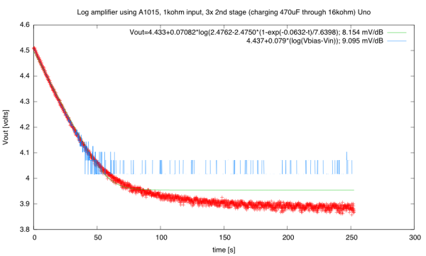
(click image to embiggen) I'm now getting a clear signal from the log amplifier even after the input voltage has gotten less than one least-significant-bit away from Vbias.  I found it difficult to fit parameters for modeling the RC charge.

(click image to embiggen) I’m now getting a clear signal from the log amplifier even after the input voltage has gotten less than one least-significant-bit away from Vbias (the blue fit). I found it difficult to fit parameters for modeling the RC charge (the green fit).

The two models I fit to the data give me somewhat different mV/dB scales, though both fit the data fairly well. The blue curve fits better up to about 65 seconds, then has quantization problems. Using that estimate of 9.8mV/dB and the 560mV range of the output, we have a dynamic range here of 57dB. There is still some flattening of the curve—we aren’t quite getting to the Vbias value, but it is pretty straight for the first 50 seconds.

Note: the parallel resistance of the capacitors would not explain the not-quite-exponential behavior we saw in the RC time constant lab, since those measurements were discharging the capacitor to zero. A parallel resistance would just change the time constant, not the final voltage.

I was using the Duemilanove board for the log-amplifier tests. I retried with the Uno board, to see if differences in the ADC linearity make a difference in the fit:

    Using the Uno Arduino board I still had trouble with the fit, and the Uno ADC seems to be noisier than the Duemilanove ADC.  The missing parts of the blue curve are where the Uno board read the input as having passed Vbias.

(click to embiggen) Using the Uno Arduino board I still had trouble with the fit, and the Uno ADC seems to be noisier than the Duemilanove ADC. The missing parts of the blue curve are where the Uno board read the input as having passed Vbias.

The 625 mV range over 250 seconds corresponds to about 69dB, assuming that the 9.1 mV/dB calibration is reasonably accurate (and 64dB if the earlier 9.8mV/dB calibration is better).
My measurements of the log amplifier do not seem to yield a very consistent mV/dB parameter, with values from 9.1mV/dB to 9.8mV/dB using just the Arduino measurements (and even less consistency when a model of RC charging is used).  I’m not sure how I can do more consistent measurements with the equipment I have.  Anyone have any ideas?
Incidentally, my son has decided not to include a microphone in his project.  The silicon MEMS mic was small enough, but the op amp chip for the analog processing was too big for the small board area he had left in his layout, and he decided that the loudness detector was not valuable enough for the board area and parts cost. I believe that his available board area shrunk a little today, because he discovered that the keep-away check had not been turned on in the Eagle design-rule checker.  Turning it on indicated that he had packed the capacitors too close in places, and he had to spread them out. (At least, I think that’s what he told me—I’ve not been following his PC board layout very closely.)
I’m still interested in learning about log amplifiers and precision rectifiers, so I’m still going to breadboard the components of the design and test them out.  I’m not sure when I’ll ever use the knowledge, since the Applied Circuits course does not cover the nonlinear behavior of pn junctions nor the forward-voltage drop of diodes (we don’t use diodes in the course).


Filed under: Circuits course, Data acquisition Tagged: Arduino, BitScope, log amplifier, loudness, op amp

Still more on log amplifiers

$
0
0

Yesterday, I spent the day testing different transistors in the log amplifier, to see whether it made much difference which transistor I used.  I wanted to test all 11 transistors in the iteadstudio assortment, the 5 PNP transistors and the 6 NPN transistors, to see if it made much difference and whether one of the transistors would give me a larger mV/dB scaling than the others.

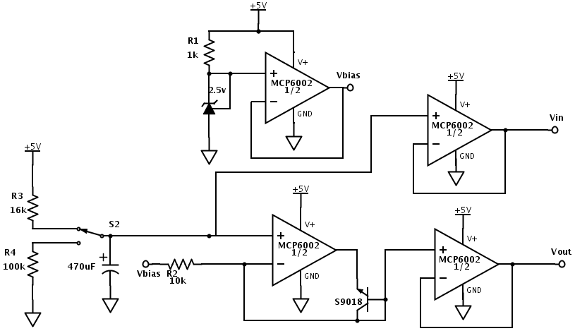
Here is the test circuit I made (essentially the same as for the tests in Logarithmic amplifier again):

The same circuit can be used for either NPN or PNP transistors.  The only difference is whether the 470µF capacitor starts at 0v (for PNP) or 5v (for NPN) before decaying to Vbias through the 16kΩ resistor.  For many of the tests the current-to-voltage resistor was 1kΩ rather than 10kΩ.

(click image to embiggen) The same circuit can be used for either NPN or PNP transistors. The only difference is whether the 470µF capacitor starts at 0v (for PNP) or 5v (for NPN) before decaying to Vbias through the 16kΩ resistor R5. For many of the tests the voltage-to-current resistor R2 was 1kΩ rather than 10kΩ.

The op amp at the top is a unity-gain buffer to provide a steady Vbias source that capable of providing some current (unlike the TL431ILP voltage reference shown here as an adjustable Zener diode). The nominal 2.5V reference was closer to 2.48V, which is within the ±2% spec for the part.

The unity-gain buffer on the left is to make the load on the RC circuit as high impedance as possible, so as not to disrupt the RC charging or discharging. The input current of the MCP6002 is typically ±1pA, which is far smaller than other sources of error (such as the parallel resistance of the capacitor itself). The parallel capacitance of the capacitor makes the destination voltage of the RC circuit slightly lower than Vbias, which means that we will not get all the way to Vbias when testing PNP transistors, but will overshoot slightly when testing NPN transistors. (We should be able to reverse that by putting the capacitor between +5V and the switch, rather than ground and the switch.)

The right-hand op amp is just a non-inverting amplifier with 3× gain, to get better precision on measuring the output voltage with the Arduino ADC.  I made some measurements with Vout but most with the 3Vout signal. The scaling factor was 3.0 much more accurately than the repeatability of my fits to the data, so the gain in precision was not accompanied by a loss of accuracy. Ideally, I’d like to be able to use more than a 3× gain in the final stage, to get better precision, but I’m limited by the offset voltage of the log amplifier, which is determined by the transistor and by the voltage-to-current converter R2.

The middle op amp is the log amplifier itself, which relies on the exponential relationship of the emitter current to the voltage across the base-emitter junction. More precisely, we can use the Ebers-Moll model of a bipolar transistor to get

i_{C} = I_{S} \left( e^{V_{BE}/V_{T}} - e^{V_{BC}/V_{T}}\right) - \frac{I_{S}}{\beta_{R}}\left( e^{V_{BE}/V_{T}} - 1\right)

The collector is held at Vbias by the feedback loop of the op amp, so VBC is zero, simplifying the equation to

i_{C} = I_{S}(1-1/\beta_{R})\left( e^{V_{BE}/V_{T}} - 1\right)

Assuming that βR and IS are constant, and that VBE is very large compared to VT (about 23 times bigger in my measurements), we have the desired exponential relationship: i_{C} \approx x e^{V_{BE}/V_{T}} for some constant x.  Note that if we leave the –1 in, then we’ll have a small DC offset to iC.

(I believe that all this analysis is correct for NPN transistors, where VBE is positive, but that some signs may need to be negated for PNP transistors.)

The log-amplifier output V_{out}-V_{bias} = -V{BE} = V_{T} \ln i_{C}- V_{T} \ln x is temperature-dependent, since V_{T} = k T /q, which is about 26mV at 300˚K. The scale factor can be multiplied by ln(10) to get 60mV/decade or 3mv/dB.

Note that this scaling is not affected by the current gain β of the transistor—that only affects the offset of the output voltage. This analysis agrees with the statement in Wikipedia, “At room temperature, an increase in VBE by approximately 60 mV increases the emitter current by a factor of 10.” There is probably an even bigger temperature dependence for the offset of the output than for the scaling, because of changes in βR and IS, but that is not included in the Ebers-Moll model.

The theoretical result indicates that I should get about 3mV/dB for any transistor, but that the offset voltage will vary depending on the characteristics of the transistor.  I might also run into effects not included in the Ebers-Moll model, especially at very large or very small collector currents.

Adjusting R2 to change the current can move the output offset around. If I make R2 large and the current small, then VBE will be small, and the approximation e^{V_{BE}/V_{T}}- 1 \approx e^{V_{BE}/V_{T}} will be poor. If I make R2 small, the current may exceed what the transistor is designed for and there may be saturation effects.

Looking at typical collector currents on the I-vs-V plots for the transistors, I’m seeing values like 8–20mA at the high end, so with a 2.5V drop across R2, I want R2 to be at least 300Ω. Initially, I picked 1kΩ, as providing a large current at 2.5V, hoping that this would give a large dynamic range.  Here are a couple of good examples of measurements using the 3× output and R2=1kΩ.

Typical 3x Vout vs Vin curve for a PNP transistor, here the A1015.  This uses Arduino-measured Vin, Vout, and Vbias, so is limited to about 2 decades (40dB).

(click image to embiggen) Typical 3× Vout vs Vin curve for a PNP transistor, here the A1015, using R2=1kΩ. This uses Arduino-measured Vin, Vout, and Vbias, so is limited to about 2 decades (40dB).

Typical 3x Vout vs. Vin curve for an NPN transistor. Again we're limited by the Arduino ADC to about 40dB of dynamic range.

(click image to embiggen) Typical 3× Vout vs. Vin curve for an NPN transistor, using R2=1kΩ. Again we’re limited by the Arduino ADC to about 40dB of dynamic range.

The exponential decay of the capacitor to about Vbias allows us to extend the range of the fit well past the resolution of the ADC to measure Vin or Vbias. Combining the formulas for the log amplifier and the RC discharge gives us the general formula
V_{out}(t) = v_{1} + v_{2} \ln( v_{3} + v_{4} e^{-t/(RC)} ).
Fitting the constants for this turns out to be difficult, because v3 is close to zero. If it were exactly zero, the formula would be v_{1} - \frac{v_{2}}{RC} t, and we could make arbitrary tradeoffs between v2 and RC.

We can get a nice plot of Vout vs. time as the capacitor decays toward Vbias, particularly for the NPN transistor S9013:

The S9013 log amplifier shows what looks like good linearity over about 80dB, when using R2=1kΩ.

(click picture to embiggen) The S9013 log amplifier shows what looks like a good fit over about 80dB, when using R2=1kΩ, and good linearity for about 65dB. The upward tail shows where the collector-base junction begins to be forward biased, and the current is no longer controlled by the base-emitter voltage.

Note that this curve shows that the problems we had with direct measurement of RC discharge curves in the physics lab was due to limitations of the Arduino ADC, not to the underlying RC circuit. The tails of the discharge continue to follow the exponential well beyond the resolution of the 10-bit ADC in the Arduino.

Of course, I picked out the S9013 plot to show, because it was the nicest one. Some of the others were weird. For example, consider the 2N5551:

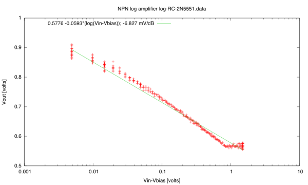
Not that the 2N5551 Vout vs Vin curve is not a simple logarithm—there is saturation happening for large input voltages.

(click image to embiggen) Not that the 2N5551 Vout vs Vin curve is not a simple logarithm—there is some sort of saturation happening for large input voltages, so the straight-line fit is awful.

The same 2N5551 transistor with R2 at 10kΩ behaves much better:

With a 10kΩ resistor, the currents through the 2N5551 transistor are smaller, and no clipping occurs.

(click image to embiggen) With a 10kΩ resistor, the currents through the 2N5551 transistor are smaller, and no clipping occurs.

Even weirder was the behavior of the S9018 NPN transistor (the only transistor in the set not matched by a corresponding PNP transistor):

With R2=1kΩ, the S9018 transistor shows a flat spot in the response for  277uA < I_C <  330uA .  I have no idea what causes this flat spot.

(click image to embiggen) With R2=1kΩ, the S9018 transistor shows a flat spot in the response for  277mV < Vin-Vbias < 330mV (that is, 277uA < IC < 330uA) . I have no idea what causes this flat spot.

I’m still mystified by the flat spot in the S9018 response—anyone have any ideas??

By changing R2 to 10kΩ, we can push the flat spot to 10× higher voltage, just outside the input range that the log amplifier uses:

With R2=10kΩ, the response of the amplifier with a S9018 transistor is nicely logarithmic.

(click image to embiggen) With R2=10kΩ, the response of the amplifier with a S9018 transistor is nicely logarithmic.

The time response to the RC discharge also looks good:

With R2=10kΩ, we get a good fit for about 76dB on the S9018 transistor.

(click to embiggen) With R2=10kΩ, we get a good fit for about 76dB on the S9018 transistor. The larger resistor gives a somewhat softer turn on for the transistor if we go past Vbias.

All of my transistors gave mV/dB scaling that was about the same (just under 9 mV/dB after the 3× gain, so just under 3mV/dB for the unamplified output), as is predicted by the Ebers-Moll model.  I got better dynamic ranges for the NPN transistors than for the PNP transistors, but this may have been due to artifacts of the test setup.  In any case, it looks like 60–70dB ranges are fairly easily achieved.

[UPDATE 2013 July 15: I know I said I was done with the log amplifiers, but I had to do just one more test.  In addition to the 16kΩ resistor to Vbias, I added a 5.7MΩ resistor to +5V, giving me a slightly higher target voltage so that I had some overshoot when testing PNP transistors.  With this setup I could test the S9012 PNP transistor for 82dB with R2=1kΩ, and 63dB with R2=10kΩ.  So the better dynamic range of the NPN was just an artifact of my test setup, as I thought.]

If one were to try to make a measuring instrument with a log amplifier, there would have to be some temperature compensation as the log-amplifier offset and scaling are both temperature sensitive.  Having a temperature-independent voltage source for calibration would be a good idea.

I think I’m about burned out on log amplifiers now.  Perhaps later his week I’ll try doing some precision rectifier circuits.


Filed under: Circuits course, Data acquisition Tagged: Arduino, bipolar transistors, log amplifier, op amp

Precision rectifier

$
0
0

The log amplifier that I’ve spent the last several days understanding (posts a, b, c) is not the only non-linear circuit needed for a loudness detector.  We also need to convert the audio input signal into a slowly changing amplitude signal that we can take the logarithm of.  As I discussed in the first post on log amps, I had rejected true-RMS converter chips as too expensive for the application (though the original application has gone away), and decided to try a rectifier and low-pass filter.

[Incidentally, my son is now looking at a different processor chip, the KL25 from Freescale (an ARM Cortex chip), which has a 16-bit ADC that is much faster than the ATMega's, so the entire loudness-detector could be done in software, except for a one-op-amp preamplifier.  With a  16-bit ADC, we can get almost 90dB of range without needing a log amplifier. We're planning to order a development board that is compatible with Arduino shields (but has lots more I/O pins available) and that has an accelerometer on the board.  Amazingly, the development board is only $13, about half the price of an Arduino.]

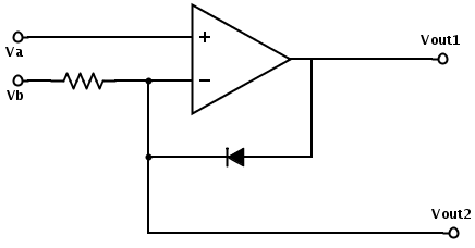
A single diode does not work for our rectifier needs in the loudness circuit, because diodes don’t turn on until the voltage across them is at least a “diode drop” (about 0.7v for silicon diodes and 0.45v for Schottky diodes).  However, the simple circuit for the log amplifier is also the circuit for a precision rectifier:

This circuit is both a log amplifier and a precision rectifier.  If Vb is set to a constant voltage, then Vout1-Vb varies as log(Vb-a).  Vout2 is max(Va,Vb).

This circuit is both a log amplifier and a precision rectifier. If Vb is set to a constant voltage, then Vout1 varies as log(Vb–Va). Vout2 is max(Va,Vb). 
The diode can be connected in the opposite direction, to get Vout2=min(Va,Vb) and Vout1 varying with log(Va–Vb).

The log-amplifier circuit I used in the previous posts had a transistor in place of the diode, so that the crucial voltage that was being exponentiated was referenced to the bias voltage, rather than the input. We also needed a compensation capacitor in parallel with the transistor to prevent oscillation in the negative feedback loop.

For the precision rectifier, we swap the inputs, so that Va is the signal input and Vb is a constant threshold voltage for the rectifier. We do not need (or want) the compensation capacitor, as that would cause the circuit to act as a unity gain amplifier at high frequency, rather than as a rectifier.

Because I did not happen to have any diodes, but had plenty of transistors, I experimented with the rectifier circuit using diode-connected bipolar transistors (collector and base connected together). Because the output of the rectifier is not directly driven by an op amp, I used unity-gain buffers to isolate the test circuitry (Arduino analog inputs or BitScope oscilloscope) from the amplifier:

Test circuit for low-speed testing of precision rectifier circuit.

Test circuit for low-speed testing of precision rectifier circuit. Here the NPN transistor is used as a diode, in the opposite direction as in the first schematic, so Vout should be min(Vin, Vbias)

My initial test setup did not have the unity-gain buffer for Vin, but I found that one of my Arduino analog input pins was quite low impedance and was discharging my capacitor. Switching to a different pin helped, but I eventually decided to avoid that kluge and use a unity-gain buffer instead.

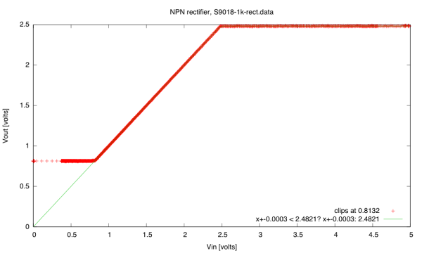
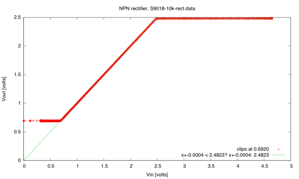
I tried several different values for R2. The most predictable effect of changing the value is a change in the range over which the rectifier operates. Clipping occurs because the output of the op amp is limited to be between the rails of the power supply. The feedback transistor is conducting when the rectifier is following the input, so the op amp output has to be substantially lower than Vout.  The function implemented is max(Vclip, min(Va,Vbias)).  Vclip should go down as R2 is increased (at about 60mV for each factor of 10 in resistance—the same shift as in the log amplifier).

Here are a couple of plots of Vout vs. Vin for the S9018 transistor:

With a 1kΩ resistor, the clipping voltage is fairly high, and we have a somewhat limited range for the rectifier.

(click to embiggen) With a 1kΩ resistor, the clipping voltage is fairly high, and we have a somewhat limited range for the rectifier.  The offset voltage for the rectifier between the output and the input is much less than the resolution of the Arduino ADC (about 5mV).

With a 10kΩ resistor, the clipping voltage is lower, giving us more range for the rectifier.

(click to embiggen) With a 10kΩ resistor, the clipping voltage is lower, giving us more range for the rectifier.

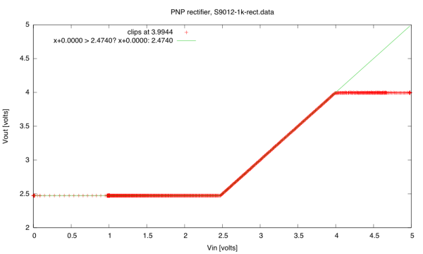
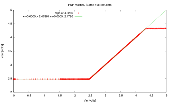
Using a PNP transistor instead of an NPN has the effect of reversing the diode and producing Vout=min(Vclip, max(Vin, Vbias)):

With an S9012 PNP transistor and a 10kΩ resistor, we get clipping at the high end.

(click to embiggen) With an S9012 PNP transistor and a 1kΩ resistor, we get clipping at the high end.

With a 10kΩ resistor we get a larger range.

(click to embiggen) With a 10kΩ resistor we get a larger range.

So why not go for a very large resistor and maximize the range? From a DC perspective this looks like a win (though it is hard to see in the limit how Vbias would affect the result if the resistance went to infinity).  Of course, the problem is with high-frequency response.  Consider the difference between the S9018 NPN transistor with a 1kΩ resistor and a 330kΩ resistor:

S9018-330kohm-1kHz

(click to embiggen) With an S9018 NPN transistor and a 330kΩ resistor at 1kHz. Note the overshoot when the rectifier shuts off.

Fairly clean signal with a S9018 NPN transistor and a 10kΩ resistor at 1kHz.

(click to embiggen) Fairly clean signal with a S9018 NPN transistor and a 10kΩ resistor at 1kHz.

With a 1kΩ resistor, there is very little overshoot as the rectifier turns off.

(click to embiggen) With a 1kΩ resistor, there is very little overshoot as the rectifier turns off, but we can see a bit of a problem when the rectifier turns back on.

There is a problem with the rectifier turning on slowly, because Vout has to move all the way from the top rail down to the bias voltage, and the op amp has a slew-rate limitation. This phenomenon can be seen more clearly at a higher frequency:

The S9018 NPN transistor with a 10kΩ resistor and a 15kHz input signal.  The overshoot as the rectifier turns off is about 50mV, and the turn-on delay is about 8µsec.  The turn-on delay does not vary much with the input resistance, unlike the turn-off overshoot.

(click to embiggen) The S9018 NPN transistor with a 10kΩ resistor and a 15kHz input signal. The overshoot as the rectifier turns off is about 50mV, and the turn-on delay is about 8µsec. The turn-on delay does not vary much with the input resistance, unlike the turn-off overshoot.

I believe that the overshoot as the rectifier turns off is due to capacitance, as adding a small feedback capacitor in parallel with the diode increases the overshoot substantially:

With a 33pF capacitor in parallel with the diode (an S9018 NPN transistor), a 10kΩ resistor,  and a 15kHz input, the overshoot goes up to about 290mV from 50mV without the capacitor.

(click to embiggen) With a 33pF capacitor in parallel with the diode (an S9018 NPN transistor), a 10kΩ resistor, and a 15kHz input, the overshoot goes up to about 290mV from 50mV without the capacitor. The turn-on delay is masked somewhat by the high-frequency feedback.

Note: the S9018 has the best high-frequency response (if you consider 15kHZ high frequency) of any of the transistors I looked, probably because it has the lowest capacitance. For example, with a 10kΩ resistor the S9013 NPN has 120mV of overshoot at 15kHz, instead of only 50mV, and the S9012 PNP has -180mV. With a 1kΩ resistor, I can’t measure the overshoot on any of these three transistors. So the limited range with a 1kΩ resistor is compensated for by the much cleaner turn-off behavior.  I should be able to get better range by using a fast-response Schottky diode instead of diode-connected transistor.

Of course, the turn-on behavior is a bigger problem and one that can’t be fixed by playing with the resistor or the diode, because the problem is with the large voltage swing needed from the op amp in order to turn on. There are standard solutions that limit the voltage swing, but I think I’ll leave that for a later blog post.


Filed under: Circuits course, Data acquisition Tagged: Arduino, BitScope, KL25, log amplifier, loudness, op amp, rectifier

Improved rectifier

$
0
0

In the Precision rectifier post, I gave the simplest circuit for making a precision rectifier:

This circuit is both a log amplifier and a precision rectifier.  If Vb is set to a constant voltage, then Vout1-Vb varies as log(Vb-a).  Vout2 is max(Va,Vb).

This circuit is both a log amplifier and a precision rectifier. If Vb is set to a constant voltage, then Vout1 varies as log(Vb–Va). Vout2 is max(Va,Vb). 
The diode can be connected in the opposite direction, to get Vout2=min(Va,Vb) and Vout1 varying with log(Va–Vb).

And I showed the problem with this circuit at “high” frequency, as the slew rate limitations of the op amp limit the turn-on time (to about 8 µs):

The S9018 NPN transistor with a 10kΩ resistor and a 15kHz input signal.  The overshoot as the rectifier turns off is about 50mV, and the turn-on delay is about 8µsec.  The turn-on delay does not vary much with the input resistance, unlike the turn-off overshoot.

(click to embiggen) The S9018 NPN transistor with a 10kΩ resistor and a 15kHz input signal. The overshoot as the rectifier turns off is about 50mV, and the turn-on delay is about 8µsec. The turn-on delay does not vary much with the input resistance, unlike the turn-off overshoot.

I also promised, “There are standard solutions that limit the voltage swing, but I think I’ll leave that for a later blog post.”  This is that post.

The textbook standard solution is to add another diode and resistor, and to configure the rectifier as an inverting amplifier (rather than a unity-gain one) when it is following the input:

Only one of D1 and D2 can be conducting.

Only one of D1 and D2 can be conducting.

This circuit has an input impedance of R1 (not the very high input impedance of the previous circuit). In this circuit, if Vin is more than Vthreshold, the output of the op amp goes low until diode D1 conducts and the negative input of the op amp is held at Vthreshold, as is Vout (with an output impdeance of R2).  If Vin is less than Vthreshold, the output of the op amp rises until D2 conducts, and the feedback circuit makes an inverting amplifier with V_{out} -V_{threshold} = \frac{-R_{2}}{R_{1}}(V_{in} - V_{threshold}).  The output impedance is very low.  Note that the difference in the output impedance for the two states is similar to the situation for the simpler circuit, and can cause problems if the output of the rectifier is fed directly to an RC filter, unless the R value for the RC filter is much larger than R2.  For the loudness circuit, we want a very large RC time constant to smooth out the ripples of the rectifier, so a large R value is not a problem.

We expect this circuit to have problems when neither D1 nor D2 is conducting—that is, as the circuit makes transitions between the rectifier being on or off.  The simple rectifier circuit only had problems with turning on (as the op amp had to slew from a rail to a diode-drop past Vthreshold), but this improved circuit has to swing two diode drops when turning on or when turning off.  The two-diode-drop swing is smaller than the

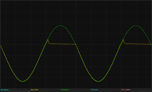
Here is an example of the output with a 30kHz clock, using S9018 transistors as diodes and R1 and R2 both at 10kΩ:

    (click to embiggen) Output (yellow) for the improved rectifier with a 30kHz triangle wave as input (green). The glitches are about 300mV and last for about 4 µsec.

(click to embiggen) Output (yellow) for the improved rectifier with a 30kHz triangle wave as input (green). The glitches are about 140mV–160mV and last for about 4 µsec.

The duration of the glitches is always about 4µs, but the magnitude of the glitches depend very much on frequency.  With a 2kHz triangle wave signal, I can’t see the glitches with the BitScope USB oscilloscope (so less than about 20mV).  The magnitude of the glitch seems to be proportional to the input magnitude. Using a constant amplitude triangle wave input (about 2.6v peak-to-peak),  I measured the glitches for some higher frequencies:

frequency positive glitch negative glitch
3kHz 40mV 40mv
10kHz 80mV 80mv
20kHz 120mV 100mv
30kHz 160mV 140mv
40kHz 200mV 180mv
50kHz 220mV 210mv
60kHz 250mV 260mv
70kHz 260mV 300mv

To understand where the glitches come from, it helps to look at the op-amp output and the negative feedback input:

The output of the op amp (green) is either a diode drop above or a diode drop below the output of the rectifier circuit.  The transitions between these states are limited by the op amp slew rate.  I measured about 600 mV/µsec, which is what the MCP6002 op amp I'm using is specified to have as a slew rate (I measured before looking it up, to keep from being biased by the correct answer).

(click to embiggen) The output of the op amp (green) is either a diode drop above or a diode drop below the output of the rectifier circuit (yellow) depending which diode is conducting.  The transitions between these states are limited by the op amp slew rate.  I measured about 600 mV/µsec, which is what the MCP6002 op amp I’m using is specified to have as a slew rate (I measured before looking it up, to keep from being biased by the “correct” answer).

 The negative input of the op amp, which the feedback circuit is trying to keep at Vthreshold, has glitches when the op amp output is ramping between its two states.

(clcik to embiggen) The negative input of the op amp (green), which the feedback circuit is trying to keep at Vthreshold, has glitches when the op amp output (yellow) is ramping between its two states.

The glitches in the improved circuit are smaller than for the simpler circuit, and can be further reduced by using Schottky diodes (to reduce the size of the diode drop, and hence how far the op amp must swing to change states) or a faster op amp (to reduce how long the op amp takes to slew the two diode drops).  I expect that with the Schottky diodes, the glitches should be reduced to 2(450mV)/(600 mV/µs)=1.5µs.  Since the glitches are basically triangular pulses, reducing the duration by a factor of 2–3 should reduce the amplitude by as much, and the total energy by 8–27.

To test the rectifier circuit with better diodes, I’ve ordered some 1N5817 Schottky diodes from Digi-key. I like dealing with that company, as they have a lot of components I need, are always very fast in processing orders, and have not yet messed up an order.  They were once out of stock on something that I had ordered, and called me up to apologize profusely for the mistake in their inventory database (normally they notify you before you order if something is out of stock).  For today’s order, they sent me notice that they had shipped the order less than an hour and a half after I had placed the order.  Because they offer first-class US mail as a shipping option, their shipping charges tend to be much less than most of the places I deal with.  (UPS ground is cheaper for big things, but no one is beating the Post Office prices on small lightweight objects.)

Disclaimer: neither Digi-key nor the Post Office has offered me anything for my endorsement—I’m just feeling pleased with them right now.


Filed under: Circuits course, Data acquisition Tagged: BitScope, Digi-key, op amp, rectifier

Improved rectifier with Schottky diodes

$
0
0

In the Improved rectifier post, I gave the following circuit for an inverting rectifier and showed traces of its performance using diode-connected S9018 NPN transistors as diodes:

Only one of D1 and D2 can be conducting.

Only one of D1 and D2 can be conducting.

With a constant amplitude triangle wave input (about 2.6v peak-to-peak),  the circuit had some pretty serious glitches:

frequency positive glitch negative glitch
3kHz 40mV 40mv
10kHz 80mV 80mv
20kHz 120mV 100mv
30kHz 160mV 140mv
40kHz 200mV 180mv
50kHz 220mV 210mv
60kHz 250mV 260mv
70kHz 260mV 300mv

I claimed that I could reduce the glitches  by replacing the NPN transistors with 1N5817 Schottky diodes.  The diodes arrived today, and I tried them out with the same 10kΩ resistors and 30kHz triangle wave as before:

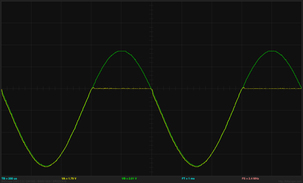
With the 1N5817 Schottky diodes, the glitches at 30kHz are much reduced—only about 68mV of overshoot.

(click to embiggen) With the 1N5817 Schottky diodes, the glitches at 30kHz are much reduced—only about 68mV of overshoot when turning off, which is half of the glitch with the S9018 NPN transistors as diodes.

I noticed that there was a bit of phase shift for the 30kHz signal, as well as the small overshoot. I tried adding capacitors in parallel with the resistors to improve the performance at 30 kHz (both to correct the phase shift and to keep the gain at -1).

This circuit works well up to 30kHz, and is still somewhat functional at 100kHz, though the "corners" have gotten soft enough that the clipping to the threshold voltage is no longer very precise at 80kHz.

This circuit works well up to 30kHz, and is still somewhat functional at 100kHz

C2 seems to adjust the overshoot, and C1 then needs to be set to fix the phase and gain.  I had the best results at 30kHz with C1=330pF and C2=220pF:

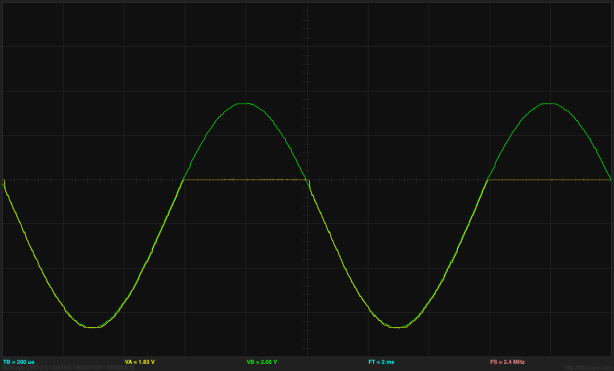
With capacitors in parallel with the feedback resistors, the phase shift is mostly corrected and there is less than 20mV of overshoot—the turn-on and turn-off corners are softened somewhat.

(click to embiggen) With capacitors in parallel with the feedback resistors, the phase shift is mostly corrected and there is less than 20mV of overshoot—the turn-on and turn-off corners are softened somewhat.

Unfortunately, there is no easy way in the BitScope software to set the offset of the traces precisely. You can do a lot of range changing and clicking the left or right sides of buttons (and start all over if you accidentally hit the middle of the button), but the offset is only displayed to 2 decimal points, but can be adjusted somewhat finer, making it hard to guess exactly what it is set to. As result, I’ve not been able to measure the overshoot or undershoot when it is less than 10mV—I’m never sure exactly what I’m measuring with respect to, and visually similar settings result in ±10mV in the estimate. In any event, the errors in this version of the improved rectifier are at least 5× better than in the version with the S9018 diode-connected transistors.

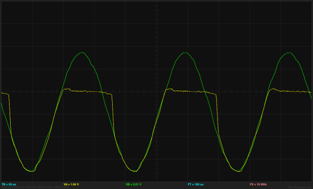
The circuit works well throughout the audio range, and can be pushed to 100kHz, though the “corners” have gotten soft enough that clipping to the threshold voltage is no longer very precise at (about 60mV off @ 80kHz—undershoot, not overshoot). At 100kHz, the output signal is still pretty good, but there is about an 85mV error in the threshold, and the corners are so rounded that the output almost looks like a sine wave:

Waveform at 100kHZ (sine wave input), showing the soft corners at that frequency.  The output doe snot get down to the threshold voltage, but only to about 85mV above threshold.

(click to embiggen) Waveform at 100kHZ (sine wave input), showing the soft corners at that frequency. The output does not get down to the threshold voltage, but only to about 85mV above threshold.

I can get better performance at 100kHz with smaller capacitors (100pF and 220pF, instead of 220pF and 330pF), but at the cost of some overshoot at 20kHz and 30kHz.  I suspect that the right values for the capacitors depend heavily on what op amp is used (especially its slew rate), but since I only have MCP6002 (and the equivalent MCP6004) op amps, I’ve not tested this suspicion.


Filed under: Circuits course, Data acquisition Tagged: BitScope, Digi-key, op amp, rectifier, Schottky diode

Virtual ground circuits

$
0
0

To use single-supply op amps properly, one usually needs to create a “virtual ground” or “bias voltage” between the two power-supply rails.  I have used 3 different circuits for these virtual grounds:

Three different virtual ground circuits I've used.

Three different virtual ground circuits I’ve used.

The circuit on the upper left is the one that I’ve been teaching in the Applied Circuits course, because it uses some of the thematic elements of the course: the voltage divider and the unity-gain buffer. The output is half the power supply voltage and tracks it well. It works well for most of the circuits they do, but has one major problem: any noise on the power-supply line is coupled into the virtual ground. Given that they could be powering their circuits off an Arduino powered from a USB port on a computer, the “5v” power can be very noisy indeed. (See, for example, the glitches observed in capacitor charging).  The unity-gain buffer limits the current from the virtual ground to about ±20mA.

The circuit on the upper right again uses a unity-gain buffer, but uses a TL431ILP  “adjustable shunt regulator” (drawn here as an adjustable zener diode).  This circuit provides a 2.5v output, as long as the power-supply voltage is high enough. The TL431ILP needs 1mA of current to get good regulation, hence the 2.5kΩ pullup resistor.  A somewhat smaller resistor would be safer, as the regulator would then have sufficient current even if the power supply voltage dropped a lot.  I usually use about a 1kΩ resistor, wasting a couple of mA to get good 2.5v output even when the input drops to 3.5v.  Without the unity-gain buffer, the shunt regulator should be able to sink about –100mA, but its source capability would limited (maybe 1.5mA with a 1kΩ pullup). We could get a balanced ±50mA capability with a 51Ω pullup, but there would be a 49mA current through the shunt regulator with no output current, resulting in 123mW of wasted power.

The bottom circuit uses a low-drop-out linear voltage regulator that can source +100mA.  This circuit is limited to sinking about –2.6mA, though, as the only path to ground is through the pair of feedback resistors, and the LDO feedback would cease to provide proper regulation once the output is pulled above the desired output voltage.  Smaller feedback resistors could be used to sink more current, at the cost of having a large current through the feedback resistors.  For example, we could get a balanced ±50mA supply by reducing the resistors to 27Ω each, but there would be a 50mA current through the feedback resistors with no output current (wasting about 116mW of power).

I don’t know of any off-the-shelf chip that provides a good voltage reference that can both source and sink significant current without wasting power in resistors.

Either the LDO or the shunt regulator costs about 40¢ (single-part costs for through-hole parts), so they are expensive parts to add to a design if not needed, but either will provide good noise immunity.


Filed under: Circuits course Tagged: op amp

Wire loop vs. twisted pair try 1

$
0
0

I was thinking about things we might do in the first lab day for the Applied Circuits course next quarter, now that I have 2 lab sessions a week.  The first, obvious thing is to unpack the lab kits and identify the different components, labeling the capacitor zip locks with values of the contained capacitors, and learning to use the wire strippers, the power supplies, and the voltmeters.

I’m thinking that I should have the students make a 3′ red-black twisted pair and pack it with their parts, so that they don’t try getting new power wires every week.

One experiment I was considering having them do is to look at the AC signal from a large loop of wire and from twisted pair, to see the difference in noise pickup.  I tried doing this at home today, with rather disappointing results.  The large loop did not pick up more 60Hz noise than the twisted pair when viewed on either my Kikusui oscilloscope or by Bitscope USB oscilloscope.  In fact I couldn’t see any noise with either one.

I tried adding my 1500-gain EKG amplifier as a front end, and then I could see about 60μV noise, but that did not change whether I used a long loop, a twisted pair, or a very short loop between the instrumentation amp inputs.

I first tried looking at how much noise there was from the Bitscope with the DP01 active probe using AC coupling:

Looking at shorted inputs  for the AC-coupled DP01 active probe in its high gain mode.  This is 2mV/division, 100µs/division, "macro" mode.  The noise is a couple of mV.

Looking at shorted inputs for the AC-coupled DP01 active probe in its high gain mode. This is 2mV/division, 100µs/division, “macro” mode. The noise is a couple of mV, about the same as the noise level without the DP01, but the resolution is much better with the DP01.  The high-speed trace here is to show the component of the noise that is around 30.8kHz, which is about as big as the 60Hz component.  The 30.8kHz noise is most likely from the USB power supply into the Bitscope.  The Bitscope does not appear to have as good power-supply noise rejection as one might want.

I then hooked up the EKG amplifier board (which should have a gain around 1508) using a separate power supply, and looked at the noise on the Vref signal (which is just buffered from a voltage divider on the power supply).

At 2mV per division and 10ms per division, we can see a little 60Hz noise added to the high-frequency noise of the Bitscope, but the noise is still only 2–3mV, which would be an input-referenced noise of about 2µV given the amplifier gain around 1500.

At 2mV per division and 10ms per division, we can see a little 60Hz noise added to the high-frequency noise of the Bitscope, but the noise is still only 2–3mV, which would be an input-referenced noise of about 2µV given the amplifier gain around 1500.

The noise on Vref is not much more than noise inherent to the Bitscope and is very similar to the noise I see looking just at the output of the power supply without the EKG attached.
Next I looked at the output of the EKG, with both inputs shorted to Vref.

This is now 40mv/division and 10ms/division looking at the output of the EKG amplifer with both inputs shorted to Vref.  The output noise is around 90mV, so the input-referenced noise is around 60µV.

This is now 40mv/division and 10ms/division looking at the output of the EKG amplifer with both inputs shorted to Vref. The output noise is around 90mV, so the input-referenced noise is around 60µV.

Now we see a signal that is not just Bitscope or power supply noise, and have a noise floor for looking at signals at the input of the EKG amplifier.

Unfortunately, replacing the short with a large loop of wire does not appreciably change the signal, but if I connect the two EKG inputs to Vref via separate 2.2MΩ resistors, I get a large output:

200mV/division, 10msec/division.  Inputs of EKG amplifier separately connected to Vref via 2.2MΩ resistors.  This signal is about 1.04V peak-to-peak (so the input is about 690µV.

200mV/division, 10msec/division. Inputs of EKG amplifier separately connected to Vref via 2.2MΩ resistors. This signal is about 1.04V peak-to-peak (so the input is about 690µV).

The output can be changed substantially by putting my hand near the resistors—the 60Hz noise appears to be capacitively coupled into the amplifier. I can reduce the peak-to-peak voltage to about 500mV  (that is around 300µV at the input) and make it have a larger 120Hz that is almost 10dB larger than the 60Hz component, , just by moving my finger around near the resistors. I can also raise the signal until the EKG amplifier is swinging rail-to-rail (at least 3mV at the input).

So I don’t have a demonstration circuit for electromagnetic pickup here, but I do have one for capacitive coupling.  To detect currents induced in a loop, I probably need a transimpedance amplifier to detect small currents, rather than an instrumentation amplifier to detect small voltages .  I’ll leave that for a separate post.


Filed under: Circuits course Tagged: BitScope, EKG, instrumentation amp, noise, op amp

More on loudness circuits

$
0
0

My son got interested in a loudness circuit again, and we tried coming up with one that that would take few components. We decided on having a 3-stage system: a preamp to get voltage up, a peak (or trough) detector with low-pass filter to extract the envelope, and a log amplifier to convert to a dB scale. We were planning to use a Schottky diode, rather than a precision rectifier for the peak detector.

Block diagram for loudness sensor using peak detector.

Block diagram for loudness sensor using peak detector.

The gain of the first stage was set by looking at the sensitivity of the SPU0410HR5H‐PB silicon microphone and the maximum loudness that the system should be able to record. The mic has -42±3dB sensitivity referenced to 1V/Pa.  That means it has 7.94mV/Pa.  The loudest sound for the mic should be the sound level at a rock concert, approximately 120dB referenced to 20µPa—that is 20Pa.  So the microphone should have an AC output of about 160mV.  Because he is planning to work with a 3.3V power supply, a gain of 10 should just keep the signal within the rails.

    Here is the loudness circuit, before the component values have been determined.

Here is the loudness circuit, before the component values have been determined.

To get a gain of 10 (actually –10), we need R2=10*R1.  The R1 C1 time constant determines the cutoff for the high-pass DC-blocking filter.  A reasonable cutoff frequency is 10–20Hz, giving an RC time constant of  8–16msec.  Picking a cheap value for C1 (0.1µF),  gives us R1≈100kΩ and R2≈1MΩ.

The peak finder is just a Schottky diode charging C2 through R3, with R4 slowly discharging it.  Because the signal does not spend a long time at the peak, we want R3≪R4, so that we can catch the peaks. We also want a moderately rapid attack (to catch percussive sounds quickly) and a fairly slow decay, so that low-pitched sounds do not appear as fluctuating loudness.  We also want R4 to be sized so that the log amplifier has a good dynamic range.  We probably want to keep the currents through Q1 to between 0.2µA and 2mA, which suggests R4≈1kΩ, and R3≈47Ω.  To make the R4*C2 time constant around 0.1 sec, C2 would have to be 100µF, which costs about 50¢, so it may be cheaper to put in another op amp to separate the peak detector from the log amplifier, using a smaller C and larger R for the peak detector, followed by an op amp, then the low resistance for the log amplifier.

Modified loudness circuit with unity-gain buffer to separate peak detector from log amplifier.

Modified loudness circuit with unity-gain buffer to separate peak detector from log amplifier.

Now we can make C2 be a reasonable size (say 0.1µF) and scale R3 and R4 to match (say 100kΩ for R4, to get a discharge time constant 0f 10msec, and 1kΩ for R3, to get a charge time constant of 100µsec).  This also limits the current drawn from U1 to 1.65mA (well less than the 15mA short-circuit current).

R5 can now be made fairly small (say 470Ω) to give us a large dynamic range on the amplifier.  If Q1 is an NPN transistor with characteristics like the S9013 transistor that I tested when I was playing with log amplifiers, then the output should range from Vref-0.65v up to almost Vref, which at 3mV/dB gives a range of over 200dB (which we certainly won’t get—the log amp may be good to 80 or 90dB.  If the ADC has 10-bit resolution on a full-scale range of Vref, then the steps are about 0.55dB (a 12-bit ADC would have steps of about 0.14dB).

Note that the log amplifier provides V_{BE} = V_{T} \ln \left ( 1+ \frac{I_{C}}{I_{SO}}\right), where IC is the collector current, ISO is the saturation current of the base-emitter diode, and VT is the thermal voltage V_{T} = \frac{k_{B} T}{q} \approx 26 mV at 300º K.  I should be able to estimate VT and ISO from the log amplifier measurements I made earlier. (I get VT =25.6mV and ISO=7.9E-15A for S9013.)

Along the way, I realized that I had never plotted a voltage-versus-current curve for the Schottky diodes, to confirm the theoretical formula V = V_{T} \ln \left ( 1+ \frac{I_{C}}{I_{S}}\right), where IS is the saturation current of the diode.

I did those measurements this morning, using a 1N5817 Schottky diode, a series resistor, a series potentiometer, and an Arduino (Leonardo) board.  I measured the voltage across the resistor (to get current) and across the diode.

The voltage does fit nicely to the log of current, with IS=1.32µA and VT=27.1 mV. Given the quantization noise in the voltage measurement, these seem like a pretty good fit to theory.

The voltage does fit nicely to the log of current, with IS=1.32µA and VT=27.1 mV. Given the quantization noise in the voltage measurement, these seem like a pretty good fit to theory. (click to embiggen)

When my son gets the Data Logger working with the KL25Z boards, I’ll probably want to redo these measurements with higher precision. Note that both VT and IS depend on temperature, and I did not measure the temperature (probably around 18ºC). IS normally doubles for every 10ºC temperature rise, so any measuring device relying on these characteristics would need to have temperature compensation or calibration to correct for temperature.  In any event the IS values for the Schottky diodes are much larger than for the base-emitter junctions, so voltage drop across the diode is much smaller for a given current—which is why we use Schottky diodes!


Filed under: Circuits course Tagged: i-vs-v-plot, log amplifier, loudness, op amp, Schottky diode

First op amp lecture

$
0
0

Today’s lecture was the first introduction of op amps to the students.  I managed to present

  • The basic notion of a differential amplifier: V_{out} = A (V_{pa} - V_{ma}).
  • Generic negative feedback amplifier.

    Generic negative-feedback amplifier design using op amps.

    Generic negative-feedback amplifier design using op amps.

  • Formula for voltage divider when none of the nodes are ground. (I had the students derive this.)
  • Formula for negative feedback with effectively infinite open-loop gain (deriving V_{out}= (V_{p}-V_{m}) Z_{f}/Z_{i} + V_{p})
  • Inverting, non-inverting, and unity-gain configurations.

I even had the students figure out how to make an amplifier with a gain of 0.5. The design they came up with was a unity-gain buffer followed by a voltage divider, though they started with a voltage-divider followed with a unity-gain buffer.  If we had had more time, I would have gotten them (eventually) to come up with a pair of inverting amplifiers.

We’ve talked about the voltage limits on Vout, and about Vp having an extremely large input impedance, but we’ve not talked about the input impedance of inverting amplifiers, about current limitations of the output nor output impedance, nor about slew rate or gain-bandwith product.

We will  talk about current limitations on Monday, since those do matter for the audio amplifier design they’ll be doing next week.


Filed under: Circuits course, Uncategorized Tagged: amplifier design, negative feedback, op amp, voltage divider

Block diagrams and audio amps

$
0
0

In today’s lecture, I introduced the notion of block diagrams as having two types of objects: functional blocks and connections between them. I emphasized that both parts were equally important, though computer programmers tended to focus more on the connections and electrical engineers more on the blocks.  I pointed out that basic action of decomposing an engineering design problem into separable subproblems was common to all forms of engineering, and so block diagrams were a common notation in almost all branches of engineering.

I also pointed out that block diagrams were only useful as a tool if they had a reasonable number of blocks (say 3–10), so that the system was broken into manageable pieces, but could still be viewed as one coherent system, not a rats’-nest of tiny components and wires.

As a class, we then developed a block diagram for and audio amplifier, starting from the overall task (sound in, louder sound out) and working our way inwards.

I spent quite a bit of time at each connection.  For example, for the sound in we talked about dB, dBA, and sound pressure levels.  I did not remember the reference value for 0dB of sound, but I have it in the lab handout (20µPa RMS).

We then talked about the sensitivity of the microphone, which we treated as a sound-to-current converter (with units being A/Pa).  I pointed out that the data sheet for the microphone we used did not give sensitivity in that form, but in dB for a reference of 1v/Pa, even though the microphone is a current output, not a voltage output device!  I explained that the data sheet used a current-to-voltage conversion of 2.2kΩ, though there is no particular reason to choose that value.  We also talked about the DC voltage or current bias needed for the microphone, which is much larger than the small AC signal.

The students realized that they needed a high-pass filter for blocking the DC, and realized (after a moment) that the voltage divider circuit meant that the input and output of the DC blocker meant that the microphone’s current output needed to be converted to a voltage.  Luckily, they’ve already designed a simple pullup resistor for current-to-voltage conversion, as well as a simple RC high-pass filter, so they should have no trouble doing so again.

We then jumped to the other end of the circuit and looked at the model for speaker.  I talked them into using the simplest possible model (just an 8Ω resistor), which is reasonable if we limit the frequency to 200Hz to 10kHz (adequate for speech, but not for music).  If we directly connected the circuit so far to the speaker, the students estimated that the signal would be less than a microwatt, so clearly not of much use for driving a 10w speaker. We also looked at the maximum voltage or current we’d want to apply to the speaker, to keep within the 10W RMS limit.

We then added a gain stage, which the students initially wanted to make a gain of about 4000.  I pointed out that voltage out of the op amp was limited to staying between the power rails, and that the MCP6004 op amps they have don’t have a very wide power supply range. I also pointed out that we did not want to exceed the current limits for the op amp, as that could clip the signals and distort them.  So they will need to choose a gain that will amplify the loudest sounds at the microphone to stay within the current limit of the op amp driving an 8Ω load.

Here is the block diagram they came up with:

Audio amplifier using an electret mic.

Audio amplifier using an electret mic.

One student asked a very good question—what do you do if you want more sound than the maximum current from the op amp? I told him that we would address that question in a later lab: the class-D power amp lab.

I told the students to flesh out their block diagram to a detailed schematic (with component values!) before tomorrow’s lab, so that they could spend the lab time building, testing, and debugging the amplifier. I think that they will try, but they will bog down somewhere in the multi-step process of designing the amplifier. I’m guessing that half of the class will have the structure right, but that no one will get reasonable values for all the components.

I have told them that I expect them to come up with expectations for what they should see at each point of their circuit, so that they can compare what they see on the oscilloscope with what they expect, and use the discrepancies to help them debug.


Filed under: Circuits course Tagged: amplifier design, audio amplifier, block diagram, electret microphone, loudspeaker, op amp

Audio amp lab

$
0
0

As I expected, no one came to lab today with their prelab homework done. There was a lot this week, as they needed to figure out the sensitivity of the microphone, decide how to bias it, figure out the AC voltage out of the microphone for 60dB sound input, add a DC-blocking filter (perhaps with a corner frequency above the resonant frequency of the loudspeaker), figure out when the amplifier would start clipping because it couldn’t drive the loudspeaker, determine the maximum gain for the amplifier, and determine the component values needed to implement all that.

Only one group finished  the design, built, and debugged their amplifier within the 3-hour lab time, but the rest are fairly close and will build and test their amplifiers on Thursday.  The group that finished today will probably work on adding either a volume control or a tone control for bonus points.

The MCP6004 op amps don’t really have the oomph to power the loudspeaker—with only about a 25mA output, they can’t do much more than 5mW into an 8Ω load. Even with an optimally matched load (maybe 240Ω?), they probably couldn’t output more than 150mW.

In a couple of weeks, we’ll do a more ambitious lab, in which the students will design and build a class-D power amplifier.  I’m a little worried about whether they’ll have the ability to work through the multiple stages of that design, since they were having a lot of trouble with the much simpler op-amp design. I might move the pressure-sensor instrumentation amp before the power amp, to give them more practice with multi-stage block diagrams before the power amp.


Filed under: Circuits course Tagged: amplifier design, audio amplifier, loudspeaker, op amp

Low-power audio amp lab completed

$
0
0

Everyone finished their audio amps yesterday and got them working, and most finished on time, though one group took a bit longer than the rest, so I was in the lab for 5 hours instead of 3. They did not keep careful notes of how they did the prelab, and could not reconstruct their thoughts, so they were very confused about why the amplifier was clipping with the loudspeaker in place, but not when it wasn’t.  I think that they eventually figured it out, with somewhat heavier hinting than I usually like to use (I was getting tired).

Each group had a different design, as they chose slightly different voltages for the power supply, hooked up the mic with either the full power supply or half the power supply for DC bias, used different pullup resistors for biasing the mic, used different combinations of R and C for their high-pass filter, and had different target gains.  I think I should point out in class how small changes in somewhat arbitrary design choices can result in rather different designs—all of which are correct.

One problem I had not anticipated, but ought to have, is that a lot students initially chose to use small resistors and large capacitors for their high-pass filters, but the filter is in parallel with the bias resistor for the microphone for AC, so if it has a low impedance, the I-to-V conversion results in a small AC signal.  This problem was noticed when one group was confused about why their AC signal was so much lower than they had expected.  It took me a while helping them debug to figure out what was going on (I generally don’t use electrolytic capacitors unless I need to, so I’d never set up a DC-blocking filter with a low impedance).  In next year’s handout, I’ll have to put in a bit more information about the need to have the RC filter be a fairly high impedance compared to the DC bias resistor, perhaps even including it in the sensitivity computation.  After seeing the problem, I did warn each group about the problem, and they all had to redo their RC filters, as they’d all chosen large C and small R.

A number of groups also used very small resistors for their feedback loops, until I suggested that using much of the current capabilities of the op amp to drive the feedback network was not leaving them much to drive the speaker.

I’ll also have to outline the steps of the sensitivity and gain computation more carefully next year, as students were not able to do it on their own without guidance.  Almost everyone ended up with too high a gain empirically, getting clipping at the loudspeaker with fairly modest sound input, but I didn’t see mistakes in their computation, and the op amps were clipping at about the expected current limit. Perhaps the input sounds were louder than we had allowed for—certainly the signal generators driving loudspeakers that we were using as sound sources were much louder than 60dBA at 1kHz, which is what the circuits were designed around.  Students did observe that without the loudspeaker the amplifiers produced nice-looking sine waves, but that adding the loudspeaker produced the clipping—some turned up the input sound to the point where they could observe the voltage clipping without the loudspeaker.  I should add a request for testing the amplifier with and without the loudspeaker next year.

Everyone did get enough gain from their amplifiers to hear sound from their loudspeakers and to get feedback squeal if they put the loudspeaker near the mic.  Not even the quickest group had the time to add a volume control or tone control circuit, so I’ll probably cut that from next year’s lab, though I’ll probably have them do adjustable gain for the class-D amplifier in 3 weeks, if only to save our ears from high-volume feedback squeal.  I’ve been wondering whether I should include a traditional large potentiometer (and not just an 18-turn trimpot) in the kits next year, so that students can have a more easily (if less precisely) adjustable resistor.  They are only about 70¢ for cheap ones, and they would make adding a gain control easier.

Students are getting fairly good at using the Tektronix TDS3054 digital oscilloscopes for making measurements, but everyone once in a while the scopes seem to get wedged in a weird mode where they don’t respond to some of the knobs (like setting the low pass filter) and the only way out we’ve found is to run “autoset”, and then reset a number of the parameters from there.  Although the scopes have some nice features, the user interface is still one of the worst I’ve encountered, with deeply layered menus covering the screen and buttons that cycle through different modes.

Measuring anything about the amplifiers was difficult, because the ambient noise in the room, particularly of other groups talking, made fairly large uncontrolled input signals.

One thing I did not expect, and still don’t have an explanation for, is that for all the groups the output seems to have been centered a little high when the loudspeaker was in the circuit, so that the op amp was at or near saturation at +150mV output even when there was no sound input.  With the gains the students were using, that would have resulted from the input voltage being around 0.1–1mV too high, which seems to be too much for any of the explanations I’ve thought of.  I did not observe this in my testing at home, but I don’t have a ±3v power supply at home, so I did not have exactly the same circuits as the students.

One group had a 50kHz triangle-wave oscillation for a while, but it went away while we were attempting to debug it, so I never found a satisfactory explanation.


Filed under: Circuits course Tagged: amplifier design, audio amplifier, loudspeaker, op amp

Second op amp lecture

$
0
0

Today’s lecture was the second one on op amps, after their audio amp lab.  I had 3 topics I wanted to cover: virtual grounds, transimpedance amplifiers, and gain-bandwidth product.  The gain-bandwidth product doesn’t really fit with the others, but they had just learned about voltage and current limitations in the audio-amp lab, and the only signals they use all quarter of high enough frequency for the gain-bandwidth product to matter are the audio signals—the heartbeat and breath pressure signals are very low frequency (DC to 20Hz bandwidth).

Before getting to the electronics part of the content, I did talk a little about the reasons I gave them such a long multi-step computation for the prelab last week, where they had to work through 8 or 9 steps to come up with the desired gain.  I explained that I knew they could do single-step problems, but that the quiz showed that they were having trouble putting their knowledge together to do two-step problems, so by giving them practice with long multistep problems, I was hoping to make two-step and three-step problems seem simple. Next week’s optical pulse monitor lab will again require a lot of steps, mostly in figuring out how much light gets through a finger.  This sort of computation (how big a physical signal is, how sensitive a sensor is, and how much gain is needed to observe and record the signal) is fundamental to the sensor interfacing that is the heart of the course, so I’m not apologizing to the students for the complexity of the task.

I started with virtual grounds, pointing out that next week’s lab would be powered off the KL25Z processor boards, which provide only 2 voltages: 3.3v and ground, so that they don’t have a symmetric power supply.  I drew a schematic for a non-inverting amplifier (gain 11, though that was irrelevant), with a 1.65v “virtual ground”, then we talked about how to get a 1.65v source.  I took the time to tell them about the existence of low-dropout voltage regulators, (LDOs)  and that those chips were how the KL25Z board produced 3.3v from the 5v power that came over the USB line.  I also told them that the LDO chips were capable of sourcing current, but not really capable of sinking current.  (I’m actually not sure whether they are incapable of sinking current—it would be possible to design a chip capable of both, with a small voltage change between the two directions of current flow to avoid excessive flow-through current.  I don’t think that chips normally have that capability, though.) I also told them that they did not have an LDO ship in their parts kits,  and challenged them to come up with another way to generate 1.65v from 3.3v.

Deer-in-the-headlights look.

After a fairly long wait, I asked them if they could produce 1.65v if they did not need to draw any current from it.

Deer-in-the-headlights look.

After a lot of random guessing, someone finally guessed “voltage divider”.  (I’ve told them almost every week that we have three concepts in the class: voltage dividers, complex impedance, and negative-feedback op amps, and they’ve been guessing voltage divider for almost every circuit question for 6 weeks, so I was surprised at how hard it was for them to see when a voltage divider would actually be appropriate.)  Once that guess was made, they quickly came up with two equal resistances.  I then showed them why sourcing or sinking current would cause the voltage to vary (by showing mismatched currents through the two resistors—I don’t know whether any of them got it though, as they seem to still be almost incapable of mapping any sort of math to the phenomena the math models).  I challenged them then to come up with a way to provide the same voltage but allow current to be drawn.  This took less time than before, with a student deciding that an amplifier was needed and remembering the unity-gain buffer from last week.

I was expecting students to have more trouble with the unity-gain buffer than with the voltage divider, because they’ve been using voltage dividers for 6 weeks, and this is the first time they’ve needed a unity-gain buffer. But it seems that recency trumps repetition in student thought—they are so inured to cram-and-forget learning strategies fostered by “unit-based” course organization that each new idea displaces all previous ones.

Almost all the useful ideas came from one student, though most of the class was participating. I’m worried that only that student is learning the material, and that I’m not reaching the rest.  (His group is usually the first to finish in lab also, no matter whom he is partnered with.)

After we had a virtual ground circuit consisting of a voltage divider and unity-gain buffer (and I reminded them of how the unity gain buffer worked), I pointed out that this virtual ground circuit was limited in the amount of current it could source or sink by the current capabilities of the op amp, which they had already encountered in seeing the difference in their audio amplifier outputs between having the 8Ω loudspeaker and not having it as a load.  For the MCP6004 chips they are using, with a 3.3v power supply, the current limit is about 15mA.

I also introduced them to another sort of voltage reference, using a Zener diode in place of the lower resistor in the voltage divider.  I think that this was a mistake though, as I may have confused them by giving them too much information.

After the virtual ground, I switched to talking about gain-bandwidth product.  I pointed out that the gain they had been getting was limited by the voltage rails and current limitations of the op amp, but that there was another limitation that affected the audio amplifier: a built-in low-pass filter that limited the open-loop gain.  I explained that the filter was there to prevent high-frequency oscillation due to stray parasitic feedback, but I did not even attempt to explain phase changes and oscillation—we’re sticking with amplitude for almost all analysis in this course, as their understanding of complex numbers is shaky enough that even that is stressing their skills.  I plotted the gain vs frequency on a log-log scale, which looks exactly like the low-pass RC filters they have seen already (at least in the range of frequencies they’ll use—there is usually a second-order effect with a steeper rolloff at frequencies above where the gain is less than 1).  I pointed out that the sloping line was proportional to 1/f, so that the gain times the frequency was constant (the gain-bandwidth product). For the MCP6004 chips, the gain-bandwidth product is 1MHz.

The gain of a negative-feedback amplifier is limited by the open-loop gain, so at 20kHz, their amplifiers could not produce a gain higher than 50.  I explained then the notion of multistage amplifiers, where each stage provides part of the gain (and possibly other functions, like filtering, level changing, or current-to-voltage conversion) as a way around the gain-bandwidth-product limitation.

We then switched to transimpedance amplifiers.  I first broke down the word into “trans-” and “impedance”, and explained that the “trans-” prefix here meant output/input (so opposite sides of the amplifier).  Since these are bioengineers, they are used to the “trans-” prefix from chemistry.  I asked them for the definition of impedance, and got the voltage/current definition from them after a few false starts.  So a transimpedance amplifier is one that provides a voltage output from a current input, and its gain is expressed in Ω (that is, volts/amps).

I pointed out that the pullup resistor in the microphone circuit that they had been using was a current-to-voltage converter, but that the voltage across the microphone varied with the current.  The microphone needs a nearly constant DC voltage across it, but the current fluctuations (around 1µA) were small compared to the DC current (around 200µA), so the voltage across the mic was nearly constant.  The devices they’ll be using next week (photodiodes and phototransistors) have essentially 0 current in the dark, so the signal is not a small fluctuation on a large DC current.  If we want to keep a nearly constant voltage across a photodiode or phototransistor, we can’t use a simple pullup.

So the transimpedance amplifier is needed not just to convert current to voltage, but to hold the bias voltage constant as the current changes.

I then tried to get the students to develop the transimpedance amplifier design from an op amp using the design goals. I started by asking them about the inputs of the op amp, trying to get them to remember that the negative-feedback circuits tried to bring the negative input to the same voltage as the positive input.  They’ve not had enough practice with op amps yet to have that useful rule of thumb easily recalled, so we ended up deriving it again.I started with asking them about what a bare op amp did.  It took a while before someone could come up with amplification of the difference between the two inputs.  I asked them what the gain was (looking for answers like “a lot” or “the open-loop gain”), but again got deer-in-the-headlight looks.  I ended up feeding them the answer to this one, as I ran out of Socratic questions to lead them to a good answer, and their guessing started getting wild.

I then asked them what keeping the output well within the power rails implied about inputs.  This took a while, but eventually one student realized that the difference has to be the output divided by the open-loop gain. (And yes, it was the same student.) So I was able to point out that a very large open-loop gain meant a very small difference in the input voltages, and that one could use as a rule of thumb that the inputs to an op amp in a negative feedback circuit was at the same voltage.

This got the student to the point where they figured out that the bias voltage could be put on the positive input and the current input whose voltage needed to be controlled on the negative input, but then they stalled again.  I pointed out that op amps were designed to have essentially no current through the input pins (about 1pA for the MCP6004 chips at room temperature), so the current on the input had to come from somewhere.  I don’t remember now whether a student suggested a connection to Vout or whether I gave them a resistor to Vout as a solution.

I then tried to get the students to figure out the behavior of the transimpedance amplifier from the current through the resistor.  They needed to realize two things:

  • That the voltage drop across the resistor was Vout-Vm
  • That the current through the resistor was the same as the current through the input port.

It took them a long time to get each of these—they kept wanting to make the voltage drop be just Vout. Physics classes do not seem to be doing a good job of getting across that notion that voltage is always a difference between two nodes in the circuit and I haven’t been able to make that an automatic response yet after 6 weeks—that must be a harder concept than I would have thought.

Even after they finally got the voltage drop right (yes, it was the same student), no one could come up with the idea that the current had to be the same as the current through the input.  I finally had to give it to them, pointing out the hint on the board—I’d drawn both currents with arrows on the board and had labeled them both “I”.  I reminded them of Kirchhoff’s Current Law, and pointed out that since no current flowed through the op-amp any current through the input port had to also be flowing through the resistor.

We then had the final formula: V_{out} = V_{p} + R I, and I could point out that the gain of the transimpedance amplifier was just the feedback impedance, R.  Since we were out of time at this point, I just mentioned two applications of transimpedance amplifiers they might have heard of—the nanopore lab and the nanopipette lab (where many bioengineers do their senior theses) both use very high gain transimpedance amplifiers (patch-clamp amplifiers) to measure currents in the 1–100pA range.

On Monday I’ll have to go over photodiodes and phototransistors, and probably repeat the transimpedance amplifier with a photodiode or phototransistor as the current source. I did direct them to do the prelab homework over the weekend, since we can’t afford to waste the entire Tuesday lab time doing the prelab as they did this week.  I’ll ask them on Monday about what results they got and where they bogged down in the computation—I expect that most of them will not have completed the prelab assignment, but I’ll be very disappointed if none of them have tried it.


Filed under: Circuits course Tagged: amplifier design, negative feedback, op amp, transimpedance amplifier, virtual ground, voltage divider

Phototransistor lab

$
0
0

Once again, no one came to lab today with their prelab homework done. There was a lot to do again this week, as they needed to figure out how much light was emitted by an LED, how much of that would get through a finger, and how much photocurrent that would induce in a phototransistor. The models they are using are pretty crude, but should be able to get within a factor of 10 of the right amount of current. I provided much more scaffolding in the handout, even doing some of the computations for them, but it doesn’t seem to have helped any.  I need to come up with some way to get students to actually do the prelab calculations—maybe collecting them as homework on Mondays?

They also had to do some quick checks to make sure that they could get an LED to light up with the amount  of current they designed for, and that the phototransistor and photodiode provided roughly expected currents in room light (and that shadowing the photodetector resulted in a change of current). A lot of the students still had serious problems with debugging (like not being able to figure out that they had put the LED in the wrong way around).

I did show the students the trick of looking at IR emitters with a digital camera to see them light up blue, but the trick did not work with one of the student’s cameras (an iPhone, don’t know which model), which apparently has an IR-blocking filter for its camera.

Only one group got as far as building their transimpedance amplifier, and then only by extending the lab to 4.5 hours instead of 3.  I suspect I’m going to have a late night on Thursday this week as well shepherding the rest of the groups through both the first-stage and second-stage of the amplifier.

I found one serious error in my handout for the lab, giving myself a REDO for the lab—the transimpedance amplifier had the + and – inputs swapped! The problem arose because I always put the – input on top, but SchemeIt puts it on the bottom, and I forgot to flip the component before wiring it up. I have already redone the handout, fixing that figure.

Tomorrow’s lecture class is supposed to be on filtering and amplifying the output of the first stage, but with only one group having finished the first stage and observed the output on the scope, this may be a difficult task to explain.  I’ll probably have to give them some numbers computed from my results, which were that I got about a 2–9nA pulse-based signal on top of a 100–150nA DC signal.

One important observation that my son made tonight was that the big pulse signals only came when I pressed my finger down with a pressure between my systolic and diastolic blood pressure.  I knew that there was a sweet spot, where I could feel my pulse, but I had not stopped to think what caused that.  Both feeling the pulse and the large change in blood volume come from stopping the flow during diastole, but allowing blood through during systole.


Filed under: Circuits course Tagged: amplifier design, op amp, phototransistor, pulse monitor, transimpedance amplifier

Mixed topics in lecture

$
0
0

Today’s lecture was a mish-mash of different topics.

Pre-lab assignments not getting done.
I asked the students for advice on how to get them (or next year’s class) to do the pre-lab assignments before coming to lab, rather than wasting lab hours doing homework that doesn’t need the fancy lab equipment. I told them some ideas I had had, and how everything I’d tried so far had not worked. The only idea they thought might work was requiring that pre-lab assignments be turned in the day before the lab, so that they would prioritize the work. I’ll have to look to see if that is feasible for any of the labs left this year.
Answer getting
I talked again about the “answer-getting” mindset, and how it wasn’t an appropriate one for engineers. The problems they’ll face in industry are open-ended ones, where there isn’t a single unique answer—no one is going to be giving them multiple-choice tests. They’ll have to come up with designs, justify their design choices, and document them well enough that someone else can maintain things after they get hit by a beer truck.
Subdividing problems
I told them that I was deliberately giving them long multi-step design problems so that they could get used to subdividing problems and tackling them a little a time. I had noticed that some of them were stopping as soon as they got to a subproblem they didn’t know how to handle, rather than leaving a symbolic value for the result and solving the other subproblems. It is a lot easier to fill in one hole in a long computation than to have to do the whole thing from scratch each time.
Engineering by design or by tinkering
There are two different styles of engineering: one which uses careful modeling and calculation to try to get a design that works correctly first time, and one that consists of making quick reasonable guesses, trying them out, and adjusting the design to correct problems. I confessed that as a hobbyist, I generally prefer design by tinkering, but most modern electronics does not lend itself to tinkering, because the parts are too small for hand soldering, so one needs to go through a more expensive PC board design and pick-and-place assembly to build a prototype. I did, accidentally, tell them a lie—I said that the MCP6004 quad op-amp chip they are using is available in a 2mm by 3mm package, but that package is for the 8-pin MCP6002 dual op-amp chip, and the smallest for the MCP6004 is 4mm by 6.4mm (substantially larger than 2 MCP6002 chips!). This week’s lab was intended to be a compromise between the two design styles, with Tuesday being engineering by design for the first stage and today and Thursday being tinkering to correct the problems of the first stage, but only one group got to the point on Tuesday of having a partly functional design that could be tweaked.
Results from stage 1
I had a student whose group had gotten stage 1 working in lab yesterday talk about what he and his partner had seen on the scope. He mentioned the voltage going very high when there was no finger blocking the light (and we talked a bit about saturation, pointing out the similarity to the loudspeaker lab, where they observed clipping from either voltage or current saturation—I even managed to tie in the chemical concept of saturated solutions). He talked about how the voltage dropped to Vref+100mV with a finger blocking the light. He mentioned the large 60Hz noise on top of this DC signal, and the tiny voltage that may have been from the pulse. I gave the students some ballpark figures for the sorts of currents that they might see from their phototransistor (based on both what the first group saw and what I had seen at home): about 90–150nA DC and about 2–10nA for the pulse.
Gain of first stage
We talked about ways to increase the gain of the first stage and the desirability of making it as big as possible without saturating at the top rail. One subject that came up (in response to a student question) was increasing the headroom by dropping the reference voltage for the transimpedance amplifier. That brought up the other constraint on that voltage—biasing the phototransistor. The spec sheet gave a VCE saturation voltage of 0.8v, and I suggested that they stay above that voltage (though I suspect that the design might work down to 0.7v since their currents are so small—something I should probably experiment with).
Need for filtering
I asked the students how to get rid of the DC bias, and by this point they all know that a high-pass filter was needed. We then discussed what sort of frequency range a heart rate might be (several were pretty clueless about this), but we eventually got to 30bm–240pbm, or 0.5Hz to 4Hz. I suggested that they might want a wider bandwidth, particularly on high end, to see the shape of the pulse as well. I talked about the need for a low-pass filter to reduce the 60Hz signal.
Synchronous sampling
With a little too much prompting, I managed to get them to come up with the idea of sampling at 60Hz, so that the 60Hz noise would be sampled at the same point on the waveform on each cycle and so be less of a problem. I also showed them that 30Hz or 20Hz would work just as well.
Active filters
Finally we got to what I had intended as today’s topic: modifying the transimpedance amplifier to include a low-pass filter. I showed them the transimpedance amplifier circuit again, and reminded them that the feedback did not need to be a simple resistor but could be a complex impedance. We drew the Bode plot for the desired gain of the amplifier using a 1/f (6dB/octave) rolloff, and I asked them how to design a complex impedance with that magnitude. They fairly quickly came up with the idea of using a resistor and capacitor, but at first they wanted to put them in series. We computed what the plot for that would be, and they decided to try parallel instead. Success! But almost out of time for the day, without talking about multi-stage filters or putting complex impedance in both arms of a voltage divider in the feedback loop for a bandpass filter.
Gnuplot boilerplate
I did give them a quick look at the boilerplate gnuplot script I wrote for them, that allows them to create models and test them out quickly with gnuplot, but I did not have time to work through an extended example of modifying the script for more complicated circuits, and I doubt that any of them will take the trouble to try it on their own.

I did not get a chance to tell them about the pressure on the finger being optimally between the systolic and diastolic blood pressure, but there should be time in lab for that tomorrow. By grasping the edge of a table lightly and gradually increasing the grip force, one can slowly increase the pressure until the finger throbs with the pulse—that is the amount of pressure you want to put on the fingertip.

I expect that I’ll be in the lab quite late with the students tomorrow, getting them to build their stage 1, tweak the feedback resistor (and capacitor) until the circuit has reasonable gain, then design and build their second stage. I’m betting that no one will have thought about what they need for the second stage, and most still won’t have a schematic even for the first stage.

On Friday, I’ll introduce instrumentation amps and strain gauges, for next week’s instrumentation amp lab. Monday will have to be class D amplifier design concepts, because Wed will be the quiz, and there is no Monday the week after next (Memorial Day), so we’ll have to develop class-D block diagram on Friday next week.


Filed under: Circuits course Tagged: active filter, answer-getting, gain, gnuplot, op amp, RC filter, tinkering, transimpedance amplifier

Instrumentation amp from op amps still fails

$
0
0

I’ve been trying to decide whether to have students build an instrumentation amp out of op amps in the circuits course.  Currently the INA126P instrumentation amp chip that I have them use is a black box to them, even though I include an explanation on the lab handout showing how it is internally a pair of op amps and 4 resistors:

Internally, the INS126P instrumentation amp is two op amps and 4 resistors.

Internally, the INS126P instrumentation amp is two op amps and 4 resistors.

I won’t repeat that presentation here (there’s a condensed, early version of it in a previous blog post).  I’ve not actually lectured on the 2-op-amp design before the instrumentation-amp lab, in class, though I did manage to talk about the 3-op-amp instrumentation amp this year (a waste of time, since they did not really process the ideas).

What I was interested in today was whether the pressure-sensor lab could be done entirely with op amps, rather than with the more expensive INA126P chip.

I decided to design an amplifier with a gain of around 200 and an output reference voltage around 0.5 v (based on a 3.3v supply), using the 2-op-amp design and MCP6004 op amps. Here is what I came up with:

This is the design I came up with and built.  It works, sort of.

This is the design I came up with and built. It works, sort of.

The amplifier amplifies and seems to have about the right gain, but there is a large DC offset on the output: about 0.24V, which translates to an input offset of about 1.2mV. I checked with a multimeter, and the negative-feedback voltages are indeed about that far apart, while the inputs from the pressure-sensor bridge are less than 40µV apart. The pressure sensor sensitivity is about 80µV/kPa/V, or 264µV/kPa with a 3.3V supply. If I use the pressure sensor with a blood-pressure cuff, I’ll want to go up to about 180mmHg or 24kPa, so the sensor output should be in the range 0–6.3mV. An offset of 1.2mV is huge!

If I remove Rgain from the circuit, the output offset drops to 20.88mV, which is 1.1mV referenced to the input (close to the 1.22mV measured at the negative feedback inputs).  Further removing R2 or R4 does not change the voltage difference between the negative-feedback inputs.  In fact removing all three of Rgain, R2, and R4, so that we have two unity-gain buffers (with 180kΩ and 10kΩ feedback resistors), still leaves the negative feedback points 1.22mV apart.  Each seems to be about 0.6mV from the corresponding positive input.

The problem is that the input offset voltage of the MCP6004 op amps is only guaranteed to be between –4.5mV and +4.5mV:  I’m lucky that the input offset voltage is under 1mV!  Even the INA126P instrumentation amps that we’ve been using have an input voltage offset of up to 250µV (150µV typical). One can obviously get better instrumentation amps, but the selection in through-hole parts is limited, and I’d have to go to an instrumentation amp costing $4.25  (LT1167CN8#PBF) instead of $2.68 to get the input offset voltage down to 20µV.

I’m going to have to rewrite the section of the book on instrumentation amps, to discuss (at least briefly) offset voltages.  I had originally thought that that the signals we were looking at were big enough that the offset voltages didn’t matter. For the INA126P, a 150µV offset would be about 0.6kPa, while the 1.22mV offset I was seeing in my homemade instrumentation amp would be about 4.6kPa.

I wonder also whether I can make an EKG circuit using this 2-op-amp instrumentation amp circuit.  The EKG already has to deal with potentially large input voltage offsets due to differing electrode-skin contacts.  In fact those offsets may be over100mV, far larger than the 1.2mV from the amplifier.  I’ll have to add another stage of amplification (after a high-pass filter), but that shouldn’t be a problem. I looked at this problem a year ago in 2-op-amp instrumentation amp and Common-mode noise in EKG, and concluded then that common-mode noise would be too large, but I’m tempted to try again, using the design here with gain 19 and a second stage with a gain of around 80 (for a combined gain around 1520), as last year I rejected the idea before actually building the circuit.


Filed under: Circuits course Tagged: EKG, instrumentation amp, offset voltage, op amp, pressure sensor

Instrumentation amp from op amps fine for EKG

$
0
0

As I mentioned in Instrumentation amp from op amps still fails, I’ve been trying to decide whether to have students build an instrumentation amp out of op amps in the circuits course.  I decided that it wouldn’t work for the pressure-sensor lab, because of the large DC offset.  One could calibrate each amplifier, either in software (by recording a a few seconds of 0 pressure difference, and subtracting a constant fit to that region from the data) or in hardware, but I’d rather they had a more straightforward experience where the DC offset was small enough to be ignored.

I conjectured that instrumentation amp built from discrete op amps would work ok for the EKG lab, though, as the EKG already has to deal with much larger input voltage offsets due to differing electrode-skin contact.  So I added a second stage  with a gain of 81 to the instrumentation amp in the previous post with a gain of 19, to get a combined gain of 1539.  I put in the high-pass filter needed to eliminate the DC offset, and a low-pass filter to reduce noise slightly (and make aliasing less of a problem).  The corner frequency is a bit high (60Hz noise is not going to be reduced much), but that may allow a better view of the fast R spike in the EKG waveform.

    The EKG circuit has four modules: a virtual ground (here set to 0.5v), an instrumentation amp, a high-pass filter to eliminate DC bias, and a second-stage non-inverting amplifier with some low-pass filtering.

The EKG circuit has four modules: a virtual ground (here set to 0.5v), an instrumentation amp, a high-pass filter to eliminate DC bias, and a second-stage non-inverting amplifier with some low-pass filtering.

The amplifier worked surprisingly well. I did sometimes have trouble with 60Hz noise, but it did not seem to be any worse than the amplifier based on the INA126P. I can remove the noise by digital filtering, though I’ve only played with that by post-processing the data files, not by designing a notch filter to run in realtime on the KL25Z (something to do when I have more time).

Here are a few traces made with EKG circuit above, feeding into the PTE20-PTE21 differential input on the KL25Z board, recorded using PteroDAQ.

This is lead I, without filtering, showing a rather disturbingly large 60Hz noise signal.

This is lead I (LA–RA), without filtering, showing a rather disturbingly large 60Hz noise signal.

This is lead I (LA-RA), showing how the digital filter cleans up the signal. This was Bessel bandpass filtered to 0.3Hz to 100Hz, followed by notch 57Hz–63Hz, followed by notch 117Hz–123Hz. Each filter was a 5th-order Bessel filter, applied first forward in time then backward in time (using scipy's filtfilt function).

This is lead I (LA–RA), showing how the digital filter cleans up the signal. This was Bessel bandpass filtered to 0.3Hz to 100Hz, followed by notch 57Hz–63Hz, followed by notch 117Hz–123Hz. Each filter was a 5th-order Bessel filter, applied first forward in time then backward in time (using scipy’s filtfilt function).

This is lead II (LL-RA), which for some reason had rather low noise even without filtering.

This is lead II (LL–RA), which for some reason had rather low noise even without filtering.

I noticed that sampling at 360Hz allowed me to see a bit more of the structure of the S and T complex than I’ve seen previously, particularly in lead II, and I can even make out a little bump of a U wave just after the T wave.

I now have to decide whether to have students do the EKG amplifier without an INA126P chip, using only op amps. The design will be fairly heavily constrained, as they’ll need to get it all working on a single MCP6004 chip, but it will justify my spending a bit more time on how instrumentation amps work.

I may redesign the blinky EKG to use a single MCP6004 chip also, which would reduce the price of that substantially.


Filed under: Circuits course Tagged: ECG, EKG, electrocardiogram, instrumentation amp, offset voltage, op amp

Soldered EKG from op amps

$
0
0

Today I decided to solder the EKG design from Instrumentation amp from op amps fine for EKG onto one of my instrumentation amp protoboards, leaving out the instrumentation amp chip—I wanted to see how much trouble it would be.  As it turned out, the build was fairly straightforward, but a little tedious. There are only dedicated spaces for 8 resistors on the board, but there are 9 resistors in the design I used, so one had to go elsewhere on the board.  I deliberately left out the low-pass filter on this implementation (eliminating one capacitor), which did not make a huge difference—I ended up with about 58µV peak-to-peak of 60Hz noise on my input signal (compared to about 40µV in the previous design with a capacitor for low-pass filtering), which is fairly small compared to the 870µV R spike or the 220µV T wave.  The 60Hz interference was large enough to interfere with the P wave and make it difficult to see whether or not there was a U wave.  Of course, these measurements were made in my bedroom/lab, which has a lot less 60Hz interference than the lab the students work in.  I’ll have to take the board into work and see how bad the interference is in that space.

Using a digital filter to remove the 60Hz noise reduced the 60Hz interference to under 100nV peak-to-peak (way lower than other noise components), producing very nice waveforms, even when sampling at 360 Hz.  I’ll probably want to include a digital filter Python script in the book so that people can see the cleaned up signals, even if there isn’t room in the course to design digital filters.

I still have to decide whether to have students do the EKG amplifier without the INA126P chip, using only op amps. Wiring up the bigger circuit takes time, and I’m not sure that 6 hours of lab will be enough time for students to debug their design and get it soldered—it took them long enough to solder the EKG with the INA126P chip, which has fewer components and fewer wires to route.  It took me quite a while to solder up the board, so it would probably take the students far too long.  Is the pedagogic value of designing and building a 2-op-amp instrumentation amp worth the time? I do want the students to end up with an EKG to take home, as it is a tangible artifact that can demo the function of.  I’m thinking that I could even drop the soldering of the pressure-sensor amp (since they don’t take home pressure sensors), and add soldering of the microphone pre-amp.  If I do that, I’ll probably want to redesign the protoboard again, making it an op-amp protoboard with no instrumentation amp slot, but with more resistor spaces.

Cutting one part that costs about $2.70 and the $1.90 thermometer might justify my switching back to the resistor assortment I used in Winter 2013:  1120 piece resistor assortment for $17.39 instead of 1280 piece resistor assortment (currently $10.65) without raising the lab fee.  Why would I want fewer resistors at a higher price? The 1120-piece assortment is 10 each of 112 values, while the 1280-piece assortment is 20 each of 64 values.  Also the 64 values don’t seem to be very repeatable from set to set, and some sets has duplicates (so only 62 or 63 different values).  The 112-value sets seem more reliably useful.  A hobbyist might be better off going one step further to the 3700-piece resistor assortment (25 each of 148 values), but I can’t justify the $31.48 price for my class. (The extra $14 would probably raise the lab fee.)


Filed under: Circuits course Tagged: ECG, EKG, electrocardiogram, instrumentation amp, op amp, protoboard, resistor assortments

Freshman design projects moderately successful

$
0
0

I just finished grading this year’s freshman design projects. I think that the projects were more successful this year than last year, in part because I kept the students focussed on electronics and programming (for which they had lab access and which I could help them debug), and in part because the projects were somewhat less ambitious.

There were two groups doing EKGs and 4 groups doing blood pressure meters.  Both EKG groups managed to demonstrate their projects working, as did one of the blood-pressure groups.  (I’m being fairly generous here about what “working” means—they had to get their electronics to work, capture the data, and plot the waveforms, but further interpretation or software was not required.)  The other three blood pressure groups did not manage to demonstrate their projects, but one of them managed to plot waveforms for the pressure measurements (without getting their high-pass filter and amplifier working for the pulse measurements).

Some things I learned for next year:

  • Tell the students what op amp to get.  A number of students picked op amps that turned out to be rather old-fashioned ones with very low input impedance (as low as 2MΩ), rather limited output ranges, and external nulling circuits. The cheap MCP6002 or MCP6004 chips would have worked better at lower cost.  In fact, I gave one group that seemed to have a good schematic (but couldn’t get their circuit to work) an MCP6002 chip, which they wired in place of the op amp they had been using, and their circuit worked immediately.  I would have done the same for other groups, but the others with poorly chosen op amps were about a week behind and did not have circuits that were that close to being functional.
  • Warn students sooner not to use FedEx.  My son’s and my experience with FedEx this year has been that they are ludicrously slow. At least one group was burned by a ridiculously long delivery time, having ordered with FedEx delivery just hours before I warned the class about them.  (The US Post Office is faster and cheaper for lightweight electronics orders from Digi-Key.)
  • Students who never ask questions in class probably don’t understand much that is going on—all the groups that successfully demonstrated their projects had at least one active participant in class.
  • Students who fail to turn in their progress report are almost certainly not going to complete the project on time—I need to be more assertive in getting them moving and demanding that they show me their schematics.  Almost everyone had errors in their schematics on their first design (and one of the successful groups went through 4 incorrect designs before getting to one that worked).  Students that are afraid to show me incorrect or incomplete work don’t get the feedback they need to correct the problems—I need to normalize errors more and insist on seeing stuff, even if it is wrong.
  • The MXP5050DP pressure sensors are very easy for students to use, though a bit pricey at $16 each.  The built-in amplifier makes doing pressure measurements with an Arduino fairly trivial (hook up the three wires of the sensor to A0, +5V, and GND).  They were a good choice for the freshman design seminar, though I’ll continue to use MPX2053DP sensors without an integrated amplifier for the applied circuits class—that assignment is intended to get students to design with an instrumentation amp and to understand a bit about strain gauges.
  • Get the students to plot stuff earlier in the quarter. One group tried installing gnuplot on a Mac in the lab in the last few hours, which did not go well for them.  They did eventually find a plotting program that they could install and run, but then did not have time to run the data they collected through the filtering program I’d written for the class.  Their signals were pretty clean, though, and the plots they produced were good even with just the RC high-pass filter in their amplifier, without digital filtering.
  • The students seemed (for the most part) pretty excited about the projects—even those whose projects didn’t quite work seem to have gotten a lot out of the lab times.  I should look in a couple of years to see how many have stuck with engineering majors (I suspect that some might switch to computer science or computer engineering, rather than sticking with bioengineering, but that’s ok).

Filed under: freshman design seminar Tagged: blood pressure monitor, EKG, FedEx, freshman design seminar, op amp, pressure sensor
Viewing all 68 articles
Browse latest View live